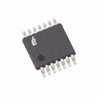
X96012V14I Intersil, X96012V14I Datasheet - Page 3

X96012V14I
Manufacturer Part Number
X96012V14I
Description
IC CNTRLR UNIV MEM/DAC 14-TSSOP
Manufacturer
Intersil
Type
Controllerr
Datasheet
1.X96012V14IZT1.pdf
(23 pages)
Specifications of X96012V14I
Input Type
*
Output Type
*
Interface
2-Wire Serial
Current - Supply
*
Mounting Type
Surface Mount
Package / Case
14-TSSOP
Lead Free Status / RoHS Status
Contains lead / RoHS non-compliant
Available stocks
Company
Part Number
Manufacturer
Quantity
Price
Company:
Part Number:
X96012V14I
Manufacturer:
Intersil
Quantity:
1 050
Part Number:
X96012V14IZ
Manufacturer:
INTERSIL
Quantity:
20 000
Electrical Specifications
Absolute Maximum Ratings
All Voltages are Referred to V
Temperature Under bias . . . . . . . . . . . . . . . . . . . . .-65°C to +100°C
Storage Temperature . . . . . . . . . . . . . . . . . . . . . . .-65°C to +150°C
Voltage on Every Pin Except VCC. . . . . . . . . . . . . . . . . -1.0V to +7V
Voltage on VCC Pin . . . . . . . . . . . . . . . . . . . . . . . . . . . . . 0V to 5.5V
DC Output Current at Pin SDA . . . . . . . . . . . . . . . . . . 0mA to 5 mA
DC Output Current at Pins R1, R2, VREF and VSENSE
DC Output Current at Pins I1 and I2 . . . . . . . . . . -3.5mA to +3.5mA
CAUTION: Do not operate at or near the maximum ratings listed for extended periods of time. Exposure to such conditions may adversely impact product reliability and
result in failures not covered by warranty
NOTE:
.
Iccstby
Iccfull
Iccwrite
I
V
V
I
V
I
V
V
VRefout
RV
TCOref
VRef Range
TSenseRange
TSenseAccuracy
PLDN
INTTL
OHSDA
1. θ
ILTTL
IHTTL
OLSDA
ILCMOS
IHCMOS
. . . . . . . . . . . . . . . . . . . . . . . . . . . . . . . . . . . . . . . -0.50mA to 1mA
REF
JA
SYMBOL
is measured with the component mounted on a high effective thermal conductivity test board in free air. See Tech Brief TB379 for details.
Stand-by Current into V
Full Operation Current into V
Pin
Nonvolatile Write Current into
V
On-chip Pull-down Current at WP,
A0, A1, and A2
SCL and SDA, Input Low Voltage
SCL and SDA, Input High Voltage
SCL and SDA Input Current
SDA Output Low Voltage
SDA Output High Current
WP, A0, A1, and A2 Input Low
Voltage
WP, A0, A1, and A2 Input High
Voltage
Output Voltage at V
VREF Pin Input Resistance
Temperature Coefficient of V
Output Voltage
Voltage Range when V
Input
Temperature Sensor Range
Temperature Sensor Accuracy
CC
Pin
SS
PARAMETER
3
Conditions are as follows, unless otherwise specified. All typical values are for T
Maximum and minimum specifications are over the recommended operating conditions. All voltages are
referred to the voltage at pin V
R
external 2kΩ resistor. 2-wire interface in “standby” (see Notes 9 and 10 on page 5). WP, A0, A1, and A2 floating.
V
REF
1
and V
pin unloaded.
REF
SS
REF
CC
at +25°C
, and another between R
Pin
is an
REF
CC
R
2-wire interface reading from
memory, I
DAC input bytes: FFh, V
Average from START condition until t
after the STOP condition
WP: V
unloaded.
V(WP), V(A0), V(A1), and V(A2) from 0V
to V
Pin voltage between 0 and V
as an input.
I(SDA) = 2mA
V(SDA) = V
-20µA ≤ I(V
VRM bit = “1”, +25°C
Notes 2 and 8
Note 6
Note 2
1
and R
CC
CC
SS
, R
2
1
X96012
TEST CONDITIONS
floating, V
. All bits in control registers are “0”. 255Ω, 0.1%, resistor connected between
and I
REF
CC
1
and R
2
) ≤ 20µA
and V
2
both connected to V
2
REF
Thermal Information
Thermal Resistance (Typical, Note 1)
Pb-free reflow profile . . . . . . . . . . . . . . . . . . . . . . . . . .see link below
Operating Conditions
Temperature Range . . . . . . . . . . . . . . . . . . . . . . . . .-40°C to +100°C
Temperature While Writing to Memory . . . . . . . . . . . . 0°C to +70°C
Voltage on V
Voltage on any other Pin . . . . . . . . . . . . . . . . . . . . . . . . . V
Floating, V
SS
14 Lead TSSOP . . . . . . . . . . . . . . . . . . . . . . . . . . . .
http://www.intersil.com/pbfree/Pb-FreeReflow.asp
. 400kHz TTL input at SCL. SDA pulled to V
REF
unloaded.
CC
unloaded.
, and SDA
REF
CC
WP
Pin . . . . . . . . . . . . . . . . . . . . . . . . . . . . . 3V to 5.5V
SS
,
0.8 x V
(Note 3)
1.205
-100
MIN
2.0
-40
20
-1
0
0
0
0
1
CC
A
TYP
1.21
+/-2
= +25°C and 5V at pin V
4
1
0.2 x V
CC
(Note 3)
1.215
MAX
+100
V
100
100
0.8
0.4
1.3
through an
15
20
10
40
2
CC
February 20, 2008
CC
θ
JA
CC
ppm/°C
FN8216.3
(°C/W)
96
UNIT
± 0.3V
mA
mA
mA
µA
µA
µA
kΩ
°C
°C
V
V
V
V
V
V
V
CC
.


