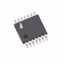
X96012V14I Intersil, X96012V14I Datasheet - Page 5

X96012V14I
Manufacturer Part Number
X96012V14I
Description
IC CNTRLR UNIV MEM/DAC 14-TSSOP
Manufacturer
Intersil
Type
Controllerr
Datasheet
1.X96012V14IZT1.pdf
(23 pages)
Specifications of X96012V14I
Input Type
*
Output Type
*
Interface
2-Wire Serial
Current - Supply
*
Mounting Type
Surface Mount
Package / Case
14-TSSOP
Lead Free Status / RoHS Status
Contains lead / RoHS non-compliant
Available stocks
Company
Part Number
Manufacturer
Quantity
Price
Company:
Part Number:
X96012V14I
Manufacturer:
Intersil
Quantity:
1 050
Part Number:
X96012V14IZ
Manufacturer:
INTERSIL
Quantity:
20 000
D/A Converter Characteristics
NOTES:
10. LSB is defined as
12. V(I1) and V(I2) are V
13. The maximum current, sink or source, can be set with an external resistor to 3.2 mA with a minimum V
.
11. Offset
A/D Converter Characteristics
I
I
t
TCO
ADCTIME
RIN
CIN
VIN
THE ADC IS MONOTONIC
Offset
FSError
DNL
INL
TempStep
Out25
9. DAC input Byte = FFh, Source or sink mode.
OVER
UNDER
rDAC
SYMBOL
SYMBOL
LSB. FSError
expressed in LSB. The Offset
a DAC is defined as the deviation between the measured and ideal incremental change in the output of the DAC, when the input changes by one
code step. It is expressed in LSB. The measured values are adjusted for Offset and Full Scale Error before calculating DNL
Integral Non-Linearity of a DAC is defined as the deviation between the measured and ideal transfer curves, after adjusting the measured transfer
curve for Offset and Full Scale Error. It is expressed in LSB.
voltage changes to 2.5V from the sourcing rail, and the current variation is < 1%.
ADC
ADC
ADC
ADC
I1I2
ADC
ADC
ADC
ADC
DAC
ADC
: The Offset of a DAC is defined as the deviation between the measured and ideal output, when the DAC input is 01h. It is expressed in
I1 or I2 Overshoot on D/A Converter Data Byte
Transition
I1 or I2 Undershoot on D/A Converter Data Byte
Transition
I1 or I2 Rise Time on D/A Converter Data Byte
Transition; 10% to 90%
Temperature Coefficient of Output Current I1 or
I2 when Using Internal Resistor Setting
DAC
A/D Converter Conversion Time
VSense Pin Input Resistance
VSense Pin Input Capacitance
VSense Input Signal Range
A/D Converter Offset Error
A/D Converter Full Scale Error
A/D Converter Differential
Nonlinearity
A/D Converter Integral Nonlinearity
Temperature Step Causing One
Step Increment of ADC Output
ADC Output at +25°C
: The Full Scale Error of a DAC is defined as the deviation between the measured and ideal output, when the input is FFh. It is
[
CC
2
3
PARAMETER
x
- 1.2V in source mode and 1.2V in sink mode. In this range the current at I1 or I2 varies < 1%.
V(VRef)
255
PARAMETER
DAC
5
is subtracted from the measured value before calculating FSError
]
divided by the resistance between R
(See “Electrical Specifications” table starting on page 3 for standard conditions). (Continued)
(See “Electrical Specifications” table starting on page 3 for standard conditions).
Proportional to A/D converter input voltage.
This value is maximum at full scale input of
A/D converter. ADCfiltOff = “1”
VSense as an input, ADCIN bit = “1”
VSense as an input, ADCIN bit = “1”,
Frequency = 1 MHz. (Note 2)
This is the A/D Converter Dynamic
Range. ADCIN bit = “1”
(Notes 2, 14)
(Note 2)
TEST CONDITIONS
DAC input byte changing from 00h to
FFh and vice versa, V(I1) and V(I2)
are V
1.2V in sink mode. (Note 2)
Bits I1FSO[1:0] ¦ 00
Bits I2FSO[1:0] ¦ 002,
VRMbit = “1”
See Figure 8
X96012
CC
TEST CONDITIONS
- 1.2V in source mode and
1
or R
2
2
to V
or
SS
.
(Note 3)
0.52
MIN
100
DAC
1
0
.DNL
(Note 3)
CC
MIN
5
= 4.5V. The compliance
DAC
01110101
: The Differential Non-Linearity of
TYP
±0.5
0.55
±1
±1
±1
±200
TYP
2
DAC
(Note 3)
V(VRef)
(Note 3)
MAX
0.58
MAX
. INL
9
7
30
0
0
February 20, 2008
DAC
: The
ppm/°C
UNIT
FN8216.3
LSB
LSB
LSB
LSB
UNIT
ms
kΩ
pF
°C
µA
µA
V
µs


