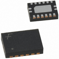
FSUSB23BQX Fairchild Semiconductor, FSUSB23BQX Datasheet

FSUSB23BQX
Specifications of FSUSB23BQX
Related parts for FSUSB23BQX
FSUSB23BQX Summary of contents
Page 1
... Cell phone, PDA, Digital Camera, and Notebook LCD Monitor, TV, and Set-Top Box Ordering Information Part Number Top Mark FSUSB23L10X EZ FSUSB23BQX USB23 MicroPak™ trademark of Fairchild Semiconductor Corporation. All packages are lead free per JEDEC: J-STD-020B standard. © 2006 Fairchild Semiconductor Corporation FSUSB23 • Rev. 1.0.1 ...
Page 2
... Figure 2. Pad Assignments for MicroPak™ (Top Through View) Pin Definitions Pin # Micropak Pin # DQFN , 12, 13 10, 11 Truth Table Sel /OE X HIGH LOW LOW HIGH LOW © 2006 Fairchild Semiconductor Corporation FSUSB23 • Rev. 1.0 GND 4 Pin Name /OE D+, D-, Dn+, Dn GND ...
Page 3
... The input and output negative voltage ratings may be exceeded if the input and output diode current ratings are observed. DC switch voltage may never exceed 4.6V. 3. The control input must be held HIGH or LOW; it must not float. © 2006 Fairchild Semiconductor Corporation FSUSB23 • Rev. 1.0.1 Parameter (1) ...
Page 4
... Output Turn-Off Time S, t OFF /OE to Output (6) t Propagation Delay PD Off Isolation, O IRR Non-Adjacent Non-Adjacent Channel Xtalk Crosstalk BW -3db Bandwidth Note: 6. Guaranteed by characterization. © 2006 Fairchild Semiconductor Corporation FSUSB23 • Rev. 1.0.1 Conditions I =-18mA ≤ Dn, D1 ≤ =0.4V, I =-8mA SW ON ...
Page 5
... Note: 7. Guaranteed by characterization. Capacitance Symbol Parameter C Control Pin Input Capacitance Capacitance Off Capacitance OFF n n © 2006 Fairchild Semiconductor Corporation FSUSB23 • Rev. 1.0.1 Conditions R =50Ω, C =10pF ( Figure 6, Figure 12 R =50Ω, C =10pF L L (7) Figure 6, Figure 12 R =50Ω, C =10pf =750ps at 480Mbps ...
Page 6
... Figure 6. AC Test Circuit Load t =2.5ns RISE V CC 90% Input - S, / 10% GND V OH 90% Output - V OUT Figure 8. Turn On / Turn Off Waveform © 2006 Fairchild Semiconductor Corporation FSUSB23 • Rev. 1.0 Select GND D1+, D1- 800mV V OUT Input GND 400mV Output:D+, D- Figure 7. Switch Propagation Delay Waveforms t =2 ...
Page 7
... Figure 10. Channel On Capacitance t =750ps RISE 800mV Input 50% 10% 400mV V OH Output:D SK(P) Pulse Skew Sel GND V Sel GND © 2006 Fairchild Semiconductor Corporation FSUSB23 • Rev. 1.0.1 S Capacitance Meter Sel CC f=1MHz t RISE 800mV Input: D =750ps FALL 400mV V 90% 90% OH 50% ...
Page 8
... Package drawings are provided as a service to customers considering Fairchild components. Drawings may change in any manner without notice. Please note the revision and/or date on the drawing and contact a Fairchild Semiconductor representative to verify or obtain the most recent revision. Package specifications do not expand the terms of Fairchild’s worldwide terms and conditions, specifically the warranty therein, which covers Fairchild products. Always visit Fairchild Semiconductor’ ...
Page 9
... Package drawings are provided as a service to customers considering Fairchild components. Drawings may change in any manner without notice. Please note the revision and/or date on the drawing and contact a Fairchild Semiconductor representative to verify or obtain the most recent revision. Package specifications do not expand the terms of Fairchild’s worldwide terms and conditions, specifically the warranty therein, which covers Fairchild products. Always visit Fairchild Semiconductor’ ...
Page 10
... Fairchild Semiconductor Corporation FSUSB23 • Rev. 1.0.1 10 www.fairchildsemi.com ...


