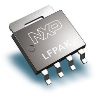
PSMN9R0-25YLC,115 NXP Semiconductors, PSMN9R0-25YLC,115 Datasheet - Page 6

PSMN9R0-25YLC,115
Manufacturer Part Number
PSMN9R0-25YLC,115
Description
MOSFET Power N-chnl25V9.1m logic lvl MOSFET in LFPAK
Manufacturer
NXP Semiconductors
Specifications of PSMN9R0-25YLC,115
Transistor Polarity
N-Channel
Resistance Drain-source Rds (on)
9.1 mOhms
Drain-source Breakdown Voltage
25 V
Gate-source Breakdown Voltage
20 V
Continuous Drain Current
46 A
Power Dissipation
34 W
Maximum Operating Temperature
+ 175 C
Mounting Style
SMD/SMT
Package / Case
LFPAK
Fall Time
5 ns
Gate Charge Qg
12 nC
Minimum Operating Temperature
- 55 C
Rise Time
10 ns
Lead Free Status / Rohs Status
Details
NXP Semiconductors
6. Characteristics
Table 6.
PSMN9R0-25YLC
Product data sheet
Symbol
Static characteristics
V
V
I
I
R
R
Dynamic characteristics
Q
Q
Q
Q
Q
V
C
C
C
t
t
t
t
DSS
GSS
d(on)
r
d(off)
f
(BR)DSS
GS(th)
GS(pl)
DSon
G
iss
oss
rss
G(tot)
GS
GS(th)
GS(th-pl)
GD
Characteristics
Parameter
drain-source breakdown
voltage
gate-source threshold voltage I
drain leakage current
gate leakage current
drain-source on-state
resistance
internal gate resistance (AC)
total gate charge
gate-source charge
pre-threshold gate-source
charge
post-threshold gate-source
charge
gate-drain charge
gate-source plateau voltage
input capacitance
output capacitance
reverse transfer capacitance
turn-on delay time
rise time
turn-off delay time
fall time
N-channel 25 V 9.1 mΩ logic level MOSFET in LFPAK using NextPower technology
All information provided in this document is subject to legal disclaimers.
Conditions
I
I
see
I
I
V
V
V
V
V
see
V
see
V
see
V
see
f = 1 MHz
I
see
I
see
I
I
see
I
see
V
T
V
R
D
D
D
D
D
D
D
D
D
D
Rev. 2 — 1 November 2011
j
DS
DS
GS
GS
GS
GS
GS
GS
DS
DS
G(ext)
= 25 °C; see
= 250 µA; V
= 250 µA; V
= 1 mA; V
= 10 mA; V
= 1 mA; V
= 15 A; V
= 15 A; V
= 0 A; V
= 15 A; V
= 15 A; V
Figure
Figure 12
Figure
Figure 12
Figure
Figure
Figure
Figure
Figure 15
= 25 V; V
= 25 V; V
= 12 V; V
= 12 V; R
= 16 V; V
= -16 V; V
= 4.5 V; I
= 4.5 V; I
= 10 V; I
= 10 V; I
= 4.7 Ω
DS
10; see
12; see
12; see
14; see
14; see
14; see
DS
DS
DS
DS
DS
DS
D
D
= 0 V; V
D
D
DS
GS
GS
GS
DS
L
GS
GS
DS
= 12 V; see
= 15 A; T
= 15 A; T
= 12 V; V
= 12 V; V
= 12 V; V
= V
= V
= 15 A; T
= 15 A; T
Figure 16
= 0.8 Ω; V
= V
= 0 V; T
= 0 V; T
= 0 V; T
= 0 V; f = 1 MHz;
= 0 V; T
= 0 V; T
= 0 V; T
GS
GS
Figure 11
Figure 13
Figure 13
Figure 15
Figure 15
Figure 15
GS
; T
; T
GS
; T
j
j
j
j
GS
GS
GS
= 10 V
j
j
j
j
j
= 25 °C;
= -55 °C
= 25 °C;
= 150 °C;
j
j
j
j
= 25 °C
= 150 °C
= 25 °C
= 25 °C;
= 150 °C;
GS
= 150 °C
= 25 °C
= -55 °C
= 25 °C
Figure
= 10 V;
= 4.5 V;
= 4.5 V;
= 4.5 V;
14;
PSMN9R0-25YLC
Min
25
22.5
1.05
0.5
-
-
-
-
-
-
-
-
-
-
-
-
-
-
-
-
-
-
-
-
-
-
-
-
-
Typ
-
-
1.6
-
-
-
-
-
-
10.5
-
7.7
-
2.35
12
5.6
10
1.8
1.2
0.6
1.8
2.7
694
205
63
13
10
16
5
© NXP B.V. 2011. All rights reserved.
-
Max
-
-
1.95
-
2.25
1
100
100
100
12.3
19.9
9.1
14.7
4.7
-
-
-
-
-
-
-
-
-
-
-
-
-
-
Unit
V
V
V
V
V
µA
µA
nA
nA
mΩ
mΩ
mΩ
mΩ
Ω
nC
nC
nC
nC
nC
nC
nC
V
pF
pF
pF
ns
ns
ns
ns
6 of 15


