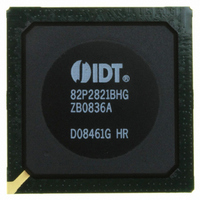
IDT82P2821BHG IDT, Integrated Device Technology Inc, IDT82P2821BHG Datasheet - Page 23

IDT82P2821BHG
Manufacturer Part Number
IDT82P2821BHG
Description
IC LINE INTERFACE UNIT 640-PBGA
Manufacturer
IDT, Integrated Device Technology Inc
Datasheet
1.IDT82P2821BHG.pdf
(151 pages)
Specifications of IDT82P2821BHG
Function
Line Interface Unit (LIU)
Interface
E1, J1, T1
Number Of Circuits
1
Voltage - Supply
1.8V, 3.3V
Operating Temperature
-40°C ~ 85°C
Mounting Type
Surface Mount
Package / Case
*
Includes
Defect and Alarm Detection, Driver Over-Current Detection and Protection, LLOS Detection, PRBSARB / IB Detection and Generation
Number Of Transceivers
1
Screening Level
Industrial
Mounting
Surface Mount
Operating Temperature (min)
-40C
Operating Temperature (max)
85C
Lead Free Status / RoHS Status
Lead free / RoHS Compliant
Current - Supply
-
Power (watts)
-
Lead Free Status / RoHS Status
Compliant, Lead free / RoHS Compliant
Other names
800-1703
82P2821BHG
82P2821BHG
Available stocks
Company
Part Number
Manufacturer
Quantity
Price
Company:
Part Number:
IDT82P2821BHG
Manufacturer:
IDT
Quantity:
170
Company:
Part Number:
IDT82P2821BHG
Manufacturer:
IDT, Integrated Device Technology Inc
Quantity:
10 000
Pin Description
IDT82P2821
VCOMEN
VCOM[0]
VCOM[1]
Name
REFA
REFB
CLKA
CLKB
REF
RIM
(Pull-Down)
(Pull-Down)
Output
Output
Output
Input
Input
Input
Input
I / O
-
Pin No.
AH17
AG17
AK18
AF26
AH10
AJ18
P28
D29
R4
REFA: Reference Clock Output A
REFA can output three kinds of clocks: a recovered clock of one of the 22 channels, an exter-
nal clock input on CLKA or a free running clock. The clock frequency is programmable. Refer
to Section 3.6.2 Clock Outputs on REFA/REFB for details.
The output on REFA can also be disabled, as determined by the REFA_EN bit (b6, REFA).
When the output is disabled, REFA is in High-Z state.
REFB: Reference Clock Output B
REFB can output a recovered clock of one of the 22 channels, an external clock input on
CLKB or a free running clock. Refer to Section 3.6.2 Clock Outputs on REFA/REFB for
details.
The output on REFB can also be disabled, as determined by the REFB_EN bit (b6, REFB).
When the output is disabled, REFB is in High-Z state.
CLKA: External T1/E1 Clock Input A
External T1/J1 (1.544 MHz) or E1 (2.048 MHz) clock is input on this pin. The CKA_T1E1 bit
(b5, REFA) should be set to match the clock frequency.
When not used, this pin should be connected to GNDD.
CLKB: External T1/E1 Clock Input B
External T1/J1 (1.544 MHz) or E1 (2.048 MHz) clock is input on this pin. The CKB_T1E1 bit
(b5, REFB) should be set to match the clock frequency.
When not used, this pin should be connected to GNDD.
VCOM: Voltage Common Mode [1:0]
These pins are used only when the receive line interface is in Receive Differential mode and
connected without a transformer (transformer-less).
To enable these pins, the VCOMEN pin must be connected high. Refer to Figure-10 for the
connection.
When these pins are not used, they should be left open.
VCOMEN: Voltage Common Mode Enable
This pin should be connected high only when the receive line interface is in Receive Differen-
tial mode and connected without a transformer (transformer-less).
When not used, this pin should be left open.
REF: Reference Resistor
An external resistor (10 KΩ, ±1%) is used to connect this pin to ground to provide a standard
reference current for internal circuit. This resistor is required to ensure correct device opera-
tion.
RIM: Receive Impedance Matching
In Receive Differential mode, when RIM is low, all 22 receivers become High-Z and only exter-
nal impedance matching is supported. In this case, the per-channel impedance matching con-
figuration bits - the R_TERM[2:0] bits (b2~0, RCF0,...) and the R120IN bit (b4, RCF0,...) - are
ignored.
In Receive Differential mode, when RIM is high, impedance matching is configured on a per-
channel basis by the R_TERM[2:0] bits (b2~0, RCF0,...) and the R120IN bit (b4, RCF0,...).
This pin can be used to control the receive impedance state for Hitless Protection applica-
tions. Refer to Section 4.4 Hitless Protection Switching (HPS) Summary for details.
In Receive Single Ended mode, this pin should be left open.
Common Control
21(+1) CHANNEL HIGH-DENSITY T1/E1/J1 LINE INTERFACE UNIT
23
Description
February 6, 2009


