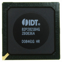
IDT82P2821BHG IDT, Integrated Device Technology Inc, IDT82P2821BHG Datasheet - Page 44

IDT82P2821BHG
Manufacturer Part Number
IDT82P2821BHG
Description
IC LINE INTERFACE UNIT 640-PBGA
Manufacturer
IDT, Integrated Device Technology Inc
Datasheet
1.IDT82P2821BHG.pdf
(151 pages)
Specifications of IDT82P2821BHG
Function
Line Interface Unit (LIU)
Interface
E1, J1, T1
Number Of Circuits
1
Voltage - Supply
1.8V, 3.3V
Operating Temperature
-40°C ~ 85°C
Mounting Type
Surface Mount
Package / Case
*
Includes
Defect and Alarm Detection, Driver Over-Current Detection and Protection, LLOS Detection, PRBSARB / IB Detection and Generation
Number Of Transceivers
1
Screening Level
Industrial
Mounting
Surface Mount
Operating Temperature (min)
-40C
Operating Temperature (max)
85C
Lead Free Status / RoHS Status
Lead free / RoHS Compliant
Current - Supply
-
Power (watts)
-
Lead Free Status / RoHS Status
Compliant, Lead free / RoHS Compliant
Other names
800-1703
82P2821BHG
82P2821BHG
Available stocks
Company
Part Number
Manufacturer
Quantity
Price
Company:
Part Number:
IDT82P2821BHG
Manufacturer:
IDT
Quantity:
170
Company:
Part Number:
IDT82P2821BHG
Manufacturer:
IDT, Integrated Device Technology Inc
Quantity:
10 000
3.5.3
3.5.3.1 Line LOS (LLOS)
monitored. When the amplitude of the data is less than Q Vpp for N
consecutive pulse intervals, LLOS is declared. When the amplitude of
the data is more than P Vpp and the average density of marks is at least
12.5% for M consecutive pulse intervals starting with a mark, LLOS is
cleared. Here Q is defined by the ALOS[2:0] bits (b6~4, LOS,...). P is the
sum of Q and 250 mVpp. N and M are defined by the LAC bit (b7,
LOS,...). Refer to Table-17 for details.
E1 mode, LLOS detection supports G.775 and ETSI 300233/I.431. The
criteria are selected by the LAC bit (b7, LOS,...).
transition from ‘0’ to ‘1’ on the LLOS_S bit (b0, STAT0,...) or any transi-
tion (from ‘0’ to ‘1’ or from ‘1’ to ‘0’) on the LLOS_S bit (b0, STAT0,...) will
set the LLOS_IS bit (b0, INTS0,...) to ‘1’, as selected by the LOS_IES bit
(b1, INTES,...). When the LLOS_IS bit (b0, INTS0,...) is ‘1’, an interrupt
will be reported by INT if not masked by the LLOS_IM bit (b0, INTM0,...).
Table-17 LLOS Criteria
Functional Description
IDT82P2821
The IDT82P2821 detects three kinds of LOS:
• LLOS: Line LOS, detected in the receive path;
• SLOS: System LOS, detected in the transmit system side;
• TLOS: Transmit LOS, detected in the transmit line side.
The amplitude and density of the data received from the line side are
In T1/J1 mode, LLOS detection supports ANSI T1.231 and I.431. In
When LLOS is detected, the LLOS_S bit (b0, STAT0,...) will be set. A
Operation
Mode
T1/J1
E1
LOSS OF SIGNAL (LOS) DETECTION
CLKE1
LLOS0
LLOS
Figure-24 LLOS Indication on Pins
LAC
0
1
0
1
CH0 CH1 CH2
One LLOS Indication Cycle
0
ETSI 300233/
ANSI T1.231
ANSI I.431
1
Criteria
G.775
I.431
2
below Q Vpp, N = 1544 bits above P Vpp, 12.5% mark density with less than 100 consecutive zeros, M = 175 bits
below Q Vpp, N = 2048 bits
below Q Vpp, N = 175 bits
below Q Vpp, N = 32 bits
CH21 CH0
21
LLOS Declaring
0
21(+1) CHANNEL HIGH-DENSITY T1/E1/J1 LINE INTERFACE UNIT
above P Vpp, 12.5% mark density with less than 100 consecutive zeros, M = 175 bits
above P Vpp, 12.5% mark density with less than 16 consecutive zeros, M = 32 bits
above P Vpp, 12.5% mark density with less than 16 consecutive zeros, M = 32 bits
44
Whether LLOS is detected in channel 0 or not, LLOS0 is high for a
CLKE1 clock cycle to indicate the channel 0 position on LLOS. LLOS
indicates LLOS status of all 22 channels in a serial format and repeats
every 22 cycles. Refer to Figure-24. LLOS0 and LLOS are updated on
the rising edge of CLKE1. When the clock output on CLKE1 is disabled,
LLOS0 and LLOS will be held in High-Z state. The output on CLKE1 is
controlled by the CLKE1_EN bit (b3, CLKG) and the CLKE1 bit (b2,
CLKG). Refer to section 8.11 on page 132 for CLKE1 timing characteris-
tics.
cated by the RMFn pin. Refer to Section 3.5.6 Error Counter and
Section 3.5.7.1 RMFn Indication respectively.
Dual Rail NRZ Format mode and Receive Dual Rail RZ Format mode,
RDn and RDPn/RDNn output low level. In Receive Dual Rail Sliced
mode RDPn/RDNn still output sliced data. RCLKn (if available) outputs
high level or XCLK
Digital Loopback is enabled, RDn, RDPn/RDNn and RCLKn output
corresponding data and clock, and the setting of the RCKH bit (b7,
RCF0,...) is ignored. Refer to the corresponding chapters for details.
Two pins (LLOS0 and LLOS) are dedicated to LLOS indication.
LLOS may be counted by an internal Error Counter or may be indi-
During LLOS, in Receive Single Rail NRZ Format mode, Receive
During LLOS, if any of AIS, pattern generation in the receive path or
1. XCLK is derived from MCLK. It is 1.544 MHz in T1/J1 mode or 2.048 MHz
in E1 mode.
1
, as selected by the RCKH bit (b7, RCF0,...).
LLOS Clearing
February 6, 2009


