IDT82P2821BHG IDT, Integrated Device Technology Inc, IDT82P2821BHG Datasheet - Page 27
IDT82P2821BHG
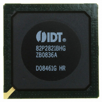
Manufacturer Part Number
IDT82P2821BHG
Description
IC LINE INTERFACE UNIT 640-PBGA
Manufacturer
IDT, Integrated Device Technology Inc
Datasheet
1.IDT82P2821BHG.pdf
(151 pages)
Specifications of IDT82P2821BHG
Function
Line Interface Unit (LIU)
Interface
E1, J1, T1
Number Of Circuits
1
Voltage - Supply
1.8V, 3.3V
Operating Temperature
-40°C ~ 85°C
Mounting Type
Surface Mount
Package / Case
*
Includes
Defect and Alarm Detection, Driver Over-Current Detection and Protection, LLOS Detection, PRBSARB / IB Detection and Generation
Number Of Transceivers
1
Screening Level
Industrial
Mounting
Surface Mount
Operating Temperature (min)
-40C
Operating Temperature (max)
85C
Lead Free Status / RoHS Status
Lead free / RoHS Compliant
Current - Supply
-
Power (watts)
-
Lead Free Status / RoHS Status
Compliant, Lead free / RoHS Compliant
Other names
800-1703
82P2821BHG
82P2821BHG
Available stocks
Company
Part Number
Manufacturer
Quantity
Price
Company:

Part Number:
IDT82P2821BHG
Manufacturer:
IDT
Quantity:
170
Company:
Part Number:
IDT82P2821BHG
Manufacturer:
IDT, Integrated Device Technology Inc
Quantity:
10 000


Pin Description
IDT82P2821
(N=0~21)
(N=0~21)
VDDRn
VDDTn
VDDIO
GNDD
VDDA
VDDD
GNDA
Name
TDO
TDI
Pull-up
Output
Input
I / O
A1, A29, A30, B1, B29, B30, F6, F7,
F8, F25, G6, G25, H6, H25, J6, J25,
P13, P14, P15, P16, P17, P18, P19,
R18, R19, T12, T13, T14, T15, T16,
V13, V14, V15, V16, V17, V18, V19,
G27, E26, E27, E5, E4, F3, F5, G3,
AD6, AD25, AE6, AE25, AJ1, AJ29,
W18, W19, AE7, AE8, AE12, AE13,
J29, F29, E29, C6, C4, C3, C2, F2,
F10, F11, F12, F13, F14, F15, F16,
F17, F18, F19, F20, F21, F22, F23,
M26, T4, W4, Y5, Y27, Y28, AA27,
U6, U25, V6, V25, W6, W25, W26,
W12, W13, W14, W15, W16, W17,
E23, E24, E25, AE9, AE10, AE15,
AF27, AD27, U27, T27, R27, N26,
AC29, AA29, Y29, R29, P29, K29,
E7, E8, E10, E11, E12, E21, E22,
N4, N5, T5, U5, AB4, AC5, AF28,
AE16, AE17, AE18, AE22, AE23,
F24, M12, M13, M14, M15, M16,
AE11, AE14, AE19, AE20, AE21
N25, P6, P25, R6, R25, T6, T25,
AB25, AB26, AC6, AC25, AC26,
M17, M18, M19, N12, N13, N14,
Y6, Y25, AA6, AA25, AB1, AB6,
K6, K25, L6, L25, M6, M25, N6,
N15, N16, N17, N18, N19, P12,
R12, R13, R14, R15, R16, R17,
U15, U16, U17, U18, U19, V12,
E14, E15, E16, E17, E18, E19,
T17, T18, T19, U12, U13, U14,
A2, B2, J26, K27, L4, L27, M4,
K2, L2, P2, R3, W2, Y2, AF29,
AJ30, AK1, AK29, AK30
AA28, AD5, AJ2, AK2
AF23, AF24
Pin No.
AE24
AF5
AF7
H3
H2
TDI: JTAG Test Data Input
The test data is input on this pin. It is clocked into the device on the rising edge of TCK. This
pin has an internal pull-up resistor.
This pin may be left unconnected when JTAG is not used.
TDO: JTAG Test Data Output
The test data is output on this pin. It is clocked out of the device on the falling edge of TCK.
TDO is a High-Z output signal except during the process of data scanning.
VDDIO: 3.3 V I/O Power Supply
VDDA: 3.3 V Analog Core Power Supply
VDDD: 1.8 V Digital Core Power Supply
VDDRn: 3.3 V Power Supply for Receiver
VDDTn: 3.3 V Power Supply for Transmitter Driver
GNDA: GND for Analog Core / Receiver
GNDD: Digital GND
Power & Ground
21(+1) CHANNEL HIGH-DENSITY T1/E1/J1 LINE INTERFACE UNIT
27
Description
February 6, 2009
Related parts for IDT82P2821BHG
Image
Part Number
Description
Manufacturer
Datasheet
Request
R

Part Number:
Description:
TRANSLATION DEVICE DPI 80-PQFP
Manufacturer:
IDT, Integrated Device Technology Inc
Datasheet:
Part Number:
Description:
IDT PART
Manufacturer:
IDT, Integrated Device Technology Inc
Datasheet:
Part Number:
Description:
IC LIU T1/E1/J1 OCTAL 256PBGA
Manufacturer:
IDT, Integrated Device Technology Inc
Datasheet:

Part Number:
Description:
IC FREQ TIMING GENERATOR 28TSSOP
Manufacturer:
IDT, Integrated Device Technology Inc
Datasheet:
Part Number:
Description:
IC CLK DVR PLL 1:10 40VFQFPN
Manufacturer:
IDT, Integrated Device Technology Inc
Datasheet:
Part Number:
Description:
IC CLK FANOUT BUFFER 1:18 32LQFP
Manufacturer:
IDT, Integrated Device Technology Inc
Datasheet:
Part Number:
Description:
IC CLK FANOUT BUFFER 1:18 32LQFP
Manufacturer:
IDT, Integrated Device Technology Inc
Datasheet:
Part Number:
Description:
IC CK505 VREG/RES 56TSSOP
Manufacturer:
IDT, Integrated Device Technology Inc
Datasheet:

Part Number:
Description:
IC SDRAM CLK DVR 1:10 48-TSSOP
Manufacturer:
IDT, Integrated Device Technology Inc
Datasheet:

Part Number:
Description:
IC CLK DVR PLL 1:10 48TSSOP
Manufacturer:
IDT, Integrated Device Technology Inc
Datasheet:
Part Number:
Description:
IC FLEXPC CLK PROGR P4 56-TSSOP
Manufacturer:
IDT, Integrated Device Technology Inc
Datasheet:
Part Number:
Description:
IC FLEXPC CLK PROGR P4 56-TSSOP
Manufacturer:
IDT, Integrated Device Technology Inc
Datasheet:
Part Number:
Description:
IC FLEXPC CLK PROGR P4 56-SSOP
Manufacturer:
IDT, Integrated Device Technology Inc
Datasheet:

Part Number:
Description:
IC PLL CLK DRIVER 2.5V 28-TSSOP
Manufacturer:
IDT, Integrated Device Technology Inc
Datasheet:
Part Number:
Description:
IC CLOCK DRIVER 2.5V 24-TSSOP
Manufacturer:
IDT, Integrated Device Technology Inc
Datasheet: