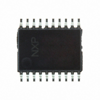
TDA1517ATW/N1,112 NXP Semiconductors, TDA1517ATW/N1,112 Datasheet - Page 10

TDA1517ATW/N1,112
Manufacturer Part Number
TDA1517ATW/N1,112
Description
IC AMP AUDIO PWR 8W STER 20TSSOP
Manufacturer
NXP Semiconductors
Type
Class Br
Datasheet
1.TDA1517ATWN1118.pdf
(19 pages)
Specifications of TDA1517ATW/N1,112
Output Type
1-Channel (Mono) or 2-Channel (Stereo)
Package / Case
20-TSSOP Exposed Pad, 20-eTSSOP, 20-HTSSOP
Max Output Power X Channels @ Load
8W x 1 @ 8 Ohm; 4W x 2 @ 4 Ohm
Voltage - Supply
6 V ~ 18 V
Features
Depop, Mute, Short-Circuit and Thermal Protection, Standby
Mounting Type
Surface Mount
Product
Class-AB
Output Power
8 W
Available Set Gain
26 dB
Thd Plus Noise
0.03 %
Operating Supply Voltage
12 V
Supply Current
40 mA
Maximum Power Dissipation
5 W
Maximum Operating Temperature
+ 85 C
Mounting Style
SMD/SMT
Audio Load Resistance
8 Ohms
Input Signal Type
Differential
Minimum Operating Temperature
- 40 C
Output Signal Type
Differential, Single
Supply Type
Single
Supply Voltage (max)
18 V
Supply Voltage (min)
6 V
Operational Class
Class-AB
Output Power (typ)
8x1@8Ohm/4x2@4OhmW
Audio Amplifier Function
Speaker
Total Harmonic Distortion
0.03@8Ohm@1W%
Single Supply Voltage (typ)
12V
Dual Supply Voltage (typ)
Not RequiredV
Power Supply Requirement
Single
Power Dissipation
5W
Rail/rail I/o Type
No
Single Supply Voltage (min)
6V
Single Supply Voltage (max)
18V
Dual Supply Voltage (min)
Not RequiredV
Dual Supply Voltage (max)
Not RequiredV
Operating Temp Range
-40C to 85C
Operating Temperature Classification
Industrial
Mounting
Surface Mount
Pin Count
20
Lead Free Status / RoHS Status
Lead free / RoHS Compliant
Lead Free Status / RoHS Status
Lead free / RoHS Compliant, Lead free / RoHS Compliant
Other names
568-3500-5
935268373112
TDA1517ATWDH
935268373112
TDA1517ATWDH
NXP Semiconductors
Thermal behaviour (PCB design considerations)
The typical thermal resistance [R
HTSSOP20 package is 37 K/W if the IC is soldered on a
printed-circuit board with double sided 35 μm copper with
a minimum area of approximately 30 cm
usable thermal resistance depends strongly on the
mounting method of the device on the printed-circuit
board, the soldering method and the area and thickness of
the copper on the printed-circuit board.
The bottom ‘heat-spreader’ of the IC has to be soldered
efficiently on the ‘thermal land’ of the copper area of the
printed-circuit board using the re-flow solder technique.
A number of thermal vias in the ‘thermal land’ provide a
thermal path to the opposite copper site of the
printed-circuit board. The size of the surface layers should
be as large as needed to dissipate the heat.
2001 Apr 17
handbook, full pagewidth
8 W BTL or 2 × 4 W SE power amplifier
R
L = 30 mm plus vias
th(j-p)
curve is given for practical calculation purpose.
Fig.5 Thermal resistance of the HTSSOP20 mounted on printed-circuit board.
K/W
60
50
40
30
20
10
0
0
th(j-a)
] of the IC in the
2
. The actual
1
number of 35 μm copper layers
2
R th(j-a)
R th(j-p)
10
3
The thermal vias (0.3 mm ∅) in the ‘thermal land’ should
not use web construction techniques, because those will
have high thermal resistance; continuous connection
completely around the via-hole is recommended.
For a maximum ambient temperature of 60 °C the
following calculation can be made: for the application at
V
dissipation approximately 2.0 W;
T
Note: the above calculation holds for application at
‘average listening level’ music output signals. Applying (or
testing) with sine wave signals will produce approximately
twice the music power dissipation; at worst case condition
this can activate the maximum temperature protection.
j(max)
P
= 12 V and R
= T
4
amb
ON-BOARD-COOLING
+ P × R
COPPER DESIGN
L
CU-LAYER 2-4
CU-LAYER 1
= 8 Ω the (ALL-) music power
th(j-a)
MGU306
L
= 60 °C + 2.0 × 37 = 134 °C.
L
TDA1517ATW
Product specification


