TDA1517ATW/N1,112 NXP Semiconductors, TDA1517ATW/N1,112 Datasheet - Page 2
TDA1517ATW/N1,112
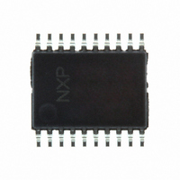
Manufacturer Part Number
TDA1517ATW/N1,112
Description
IC AMP AUDIO PWR 8W STER 20TSSOP
Manufacturer
NXP Semiconductors
Type
Class Br
Datasheet
1.TDA1517ATWN1118.pdf
(19 pages)
Specifications of TDA1517ATW/N1,112
Output Type
1-Channel (Mono) or 2-Channel (Stereo)
Package / Case
20-TSSOP Exposed Pad, 20-eTSSOP, 20-HTSSOP
Max Output Power X Channels @ Load
8W x 1 @ 8 Ohm; 4W x 2 @ 4 Ohm
Voltage - Supply
6 V ~ 18 V
Features
Depop, Mute, Short-Circuit and Thermal Protection, Standby
Mounting Type
Surface Mount
Product
Class-AB
Output Power
8 W
Available Set Gain
26 dB
Thd Plus Noise
0.03 %
Operating Supply Voltage
12 V
Supply Current
40 mA
Maximum Power Dissipation
5 W
Maximum Operating Temperature
+ 85 C
Mounting Style
SMD/SMT
Audio Load Resistance
8 Ohms
Input Signal Type
Differential
Minimum Operating Temperature
- 40 C
Output Signal Type
Differential, Single
Supply Type
Single
Supply Voltage (max)
18 V
Supply Voltage (min)
6 V
Operational Class
Class-AB
Output Power (typ)
8x1@8Ohm/4x2@4OhmW
Audio Amplifier Function
Speaker
Total Harmonic Distortion
0.03@8Ohm@1W%
Single Supply Voltage (typ)
12V
Dual Supply Voltage (typ)
Not RequiredV
Power Supply Requirement
Single
Power Dissipation
5W
Rail/rail I/o Type
No
Single Supply Voltage (min)
6V
Single Supply Voltage (max)
18V
Dual Supply Voltage (min)
Not RequiredV
Dual Supply Voltage (max)
Not RequiredV
Operating Temp Range
-40C to 85C
Operating Temperature Classification
Industrial
Mounting
Surface Mount
Pin Count
20
Lead Free Status / RoHS Status
Lead free / RoHS Compliant
Lead Free Status / RoHS Status
Lead free / RoHS Compliant, Lead free / RoHS Compliant
Other names
568-3500-5
935268373112
TDA1517ATWDH
935268373112
TDA1517ATWDH


NXP Semiconductors
FEATURES
• Requires very few external components
• Flexibility in use: mono Bridge-Tied Load (BTL) and
• High output power
• Low offset voltage at output (important for BTL)
• Fixed gain
• Good ripple rejection
• Mode select switch (operating, mute and standby)
• AC and DC short-circuit safe to ground and V
QUICK REFERENCE DATA
ORDERING INFORMATION
2001 Apr 17
V
I
I
I
SE application
P
SVRR
α
V
⎪Z
BTL application
P
SVRR
⎪ΔV
V
⎪Z
TDA1517ATW
ORM
q(tot)
stb
stereo Single-Ended (SE); it should be noted that in
stereo applications the outputs of both amplifiers are in
opposite phase
cs
P
o
n(o)
o
n(o)(offset)
8 W BTL or 2 × 4 W SE power amplifier
i
i
NUMBER
SYMBOL
⎪
⎪
OO
TYPE
⎪
supply voltage
repetitive peak output current
total quiescent current
standby current
output power
supply voltage ripple rejection
channel separation
noise output voltage
input impedance
output power
supply voltage ripple rejection
output offset voltage
noise output offset voltage
input impedance
HTSSOP20
NAME
PARAMETER
plastic thermal enhanced thin shrink small outline package;
20 leads; body width 4.4 mm; exposed die pad
P
THD = 10%; R
R
R
R
THD = 10%; R
R
R
S
S
S
S
S
2
DESCRIPTION
= 0 Ω
= 10 kΩ
= 0 Ω
= 0 Ω
= 0 Ω
• Electrostatic discharge protection
• Thermal protection
• Reverse polarity safe
• Capable of handling high energy on outputs (V
• No switch-on/switch-off plop
• Low thermal resistance.
GENERAL DESCRIPTION
The TDA1517ATW is an integrated class-AB output
amplifier contained in a plastic heatsink thin shrink small
outline package (HTSSOP20). The device is primarily
developed for multimedia applications.
PACKAGE
CONDITIONS
L
L
= 4 Ω
= 8 Ω
6
−
−
−
−
46
40
−
50
−
50
−
−
25
MIN.
TDA1517ATW
12
−
40
0.1
4
−
55
50
−
8
−
−
70
−
TYP.
Product specification
18
2.5
80
100
−
−
−
−
−
−
−
150
−
−
MAX.
SOT527-1
VERSION
P
V
A
mA
μA
W
dB
dB
μV
kΩ
W
dB
mV
μV
kΩ
= 0 V)
UNIT
Related parts for TDA1517ATW/N1,112
Image
Part Number
Description
Manufacturer
Datasheet
Request
R

Part Number:
Description:
Manufacturer:
NXP Semiconductors
Datasheet:

Part Number:
Description:
AMP, AUDIO, PWR, 8W, STER, 20TSSOP
Manufacturer:
NXP Semiconductors
Datasheet:

Part Number:
Description:
IC AMP AUDIO PWR 8W STER 20TSSOP
Manufacturer:
NXP Semiconductors
Datasheet:
Part Number:
Description:
8 W Btl Or 2 X 4 W Se Power Amplifier
Manufacturer:
NXP Semiconductors
Datasheet:

Part Number:
Description:
Audio Amplifiers 8W BTL.M. MEDIA AMP
Manufacturer:
NXP Semiconductors
Datasheet:
Part Number:
Description:
Audio Amplifiers W BTL/2X4 W SE AMP
Manufacturer:
NXP Semiconductors
Datasheet:

Part Number:
Description:
IC AMP AUDIO PWR 6W MONO B 9SIL
Manufacturer:
NXP Semiconductors
Datasheet:

Part Number:
Description:
AMP, STEREO 2 X 6W, SIL9MPF-9, 1517
Manufacturer:
NXP Semiconductors
Datasheet:
Part Number:
Description:
Manufacturer:
NXP Semiconductors
Datasheet:
Part Number:
Description:
2 X 6 W Stereo Power Amplifier
Manufacturer:
NXP Semiconductors
Datasheet:
Part Number:
Description:
NXP Semiconductors designed the LPC2420/2460 microcontroller around a 16-bit/32-bitARM7TDMI-S CPU core with real-time debug interfaces that include both JTAG andembedded trace
Manufacturer:
NXP Semiconductors
Datasheet:

Part Number:
Description:
NXP Semiconductors designed the LPC2458 microcontroller around a 16-bit/32-bitARM7TDMI-S CPU core with real-time debug interfaces that include both JTAG andembedded trace
Manufacturer:
NXP Semiconductors
Datasheet:
Part Number:
Description:
NXP Semiconductors designed the LPC2468 microcontroller around a 16-bit/32-bitARM7TDMI-S CPU core with real-time debug interfaces that include both JTAG andembedded trace
Manufacturer:
NXP Semiconductors
Datasheet:
Part Number:
Description:
NXP Semiconductors designed the LPC2470 microcontroller, powered by theARM7TDMI-S core, to be a highly integrated microcontroller for a wide range ofapplications that require advanced communications and high quality graphic displays
Manufacturer:
NXP Semiconductors
Datasheet:
Part Number:
Description:
NXP Semiconductors designed the LPC2478 microcontroller, powered by theARM7TDMI-S core, to be a highly integrated microcontroller for a wide range ofapplications that require advanced communications and high quality graphic displays
Manufacturer:
NXP Semiconductors
Datasheet: