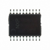
TDA1517ATW/N1,112 NXP Semiconductors, TDA1517ATW/N1,112 Datasheet - Page 4

TDA1517ATW/N1,112
Manufacturer Part Number
TDA1517ATW/N1,112
Description
IC AMP AUDIO PWR 8W STER 20TSSOP
Manufacturer
NXP Semiconductors
Type
Class Br
Datasheet
1.TDA1517ATWN1118.pdf
(19 pages)
Specifications of TDA1517ATW/N1,112
Output Type
1-Channel (Mono) or 2-Channel (Stereo)
Package / Case
20-TSSOP Exposed Pad, 20-eTSSOP, 20-HTSSOP
Max Output Power X Channels @ Load
8W x 1 @ 8 Ohm; 4W x 2 @ 4 Ohm
Voltage - Supply
6 V ~ 18 V
Features
Depop, Mute, Short-Circuit and Thermal Protection, Standby
Mounting Type
Surface Mount
Product
Class-AB
Output Power
8 W
Available Set Gain
26 dB
Thd Plus Noise
0.03 %
Operating Supply Voltage
12 V
Supply Current
40 mA
Maximum Power Dissipation
5 W
Maximum Operating Temperature
+ 85 C
Mounting Style
SMD/SMT
Audio Load Resistance
8 Ohms
Input Signal Type
Differential
Minimum Operating Temperature
- 40 C
Output Signal Type
Differential, Single
Supply Type
Single
Supply Voltage (max)
18 V
Supply Voltage (min)
6 V
Operational Class
Class-AB
Output Power (typ)
8x1@8Ohm/4x2@4OhmW
Audio Amplifier Function
Speaker
Total Harmonic Distortion
0.03@8Ohm@1W%
Single Supply Voltage (typ)
12V
Dual Supply Voltage (typ)
Not RequiredV
Power Supply Requirement
Single
Power Dissipation
5W
Rail/rail I/o Type
No
Single Supply Voltage (min)
6V
Single Supply Voltage (max)
18V
Dual Supply Voltage (min)
Not RequiredV
Dual Supply Voltage (max)
Not RequiredV
Operating Temp Range
-40C to 85C
Operating Temperature Classification
Industrial
Mounting
Surface Mount
Pin Count
20
Lead Free Status / RoHS Status
Lead free / RoHS Compliant
Lead Free Status / RoHS Status
Lead free / RoHS Compliant, Lead free / RoHS Compliant
Other names
568-3500-5
935268373112
TDA1517ATWDH
935268373112
TDA1517ATWDH
NXP Semiconductors
PINNING
FUNCTIONAL DESCRIPTION
The TDA1517ATW contains two identical amplifiers with differential input stages. This device can be used for Bridge-Tied
Load (BTL) or Single-Ended (SE) applications. The gain of each amplifier is fixed at 20 dB. A special feature of this
device is the mode select switch. Since this pin has a very low input current (<40 μA), a low cost supply switch can be
used. With this switch the TDA1517ATW can be switched into three modes:
• Standby: low supply current
• Mute: input signal suppressed
• Operating: normal on condition.
2001 Apr 17
n.c.
n.c.
IN1+
SGND
SVRR
n.c.
n.c.
OUT1a
OUT1b
PGND1
PGND2
OUT2a
OUT2b
n.c.
V
V
MODE
IN2−
n.c.
n.c.
SYMBOL
P1
P2
8 W BTL or 2 × 4 W SE power amplifier
PIN
10
12
13
14
15
16
17
18
19
20
11
1
2
3
4
5
6
7
8
9
not connected
not connected
non-inverting input 1
signal ground
supply voltage ripple rejection
not connected
not connected
output 1a
output 1b
power ground 1
power ground 2
output 2a
output 2b
not connected
supply voltage 1
supply voltage 2
mode select switch
inverting input 2
not connected
not connected
DESCRIPTION
4
handbook, halfpage
PGND1
OUT1a
OUT1b
SGND
SVRR
IN1+
n.c.
n.c.
n.c.
n.c.
Fig.2 Pin configuration.
10
1
2
3
4
5
6
7
8
9
TDA1517ATW
MGU302
TDA1517ATW
20
19
18
17
16
15
14
13
12
11
Product specification
n.c.
n.c.
IN2−
MODE
V P2
V P1
n.c.
OUT2b
OUT2a
PGND2


