TDA1517ATW/N1,112 NXP Semiconductors, TDA1517ATW/N1,112 Datasheet - Page 9
TDA1517ATW/N1,112
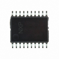
Manufacturer Part Number
TDA1517ATW/N1,112
Description
IC AMP AUDIO PWR 8W STER 20TSSOP
Manufacturer
NXP Semiconductors
Type
Class Br
Datasheet
1.TDA1517ATWN1118.pdf
(19 pages)
Specifications of TDA1517ATW/N1,112
Output Type
1-Channel (Mono) or 2-Channel (Stereo)
Package / Case
20-TSSOP Exposed Pad, 20-eTSSOP, 20-HTSSOP
Max Output Power X Channels @ Load
8W x 1 @ 8 Ohm; 4W x 2 @ 4 Ohm
Voltage - Supply
6 V ~ 18 V
Features
Depop, Mute, Short-Circuit and Thermal Protection, Standby
Mounting Type
Surface Mount
Product
Class-AB
Output Power
8 W
Available Set Gain
26 dB
Thd Plus Noise
0.03 %
Operating Supply Voltage
12 V
Supply Current
40 mA
Maximum Power Dissipation
5 W
Maximum Operating Temperature
+ 85 C
Mounting Style
SMD/SMT
Audio Load Resistance
8 Ohms
Input Signal Type
Differential
Minimum Operating Temperature
- 40 C
Output Signal Type
Differential, Single
Supply Type
Single
Supply Voltage (max)
18 V
Supply Voltage (min)
6 V
Operational Class
Class-AB
Output Power (typ)
8x1@8Ohm/4x2@4OhmW
Audio Amplifier Function
Speaker
Total Harmonic Distortion
0.03@8Ohm@1W%
Single Supply Voltage (typ)
12V
Dual Supply Voltage (typ)
Not RequiredV
Power Supply Requirement
Single
Power Dissipation
5W
Rail/rail I/o Type
No
Single Supply Voltage (min)
6V
Single Supply Voltage (max)
18V
Dual Supply Voltage (min)
Not RequiredV
Dual Supply Voltage (max)
Not RequiredV
Operating Temp Range
-40C to 85C
Operating Temperature Classification
Industrial
Mounting
Surface Mount
Pin Count
20
Lead Free Status / RoHS Status
Lead free / RoHS Compliant
Lead Free Status / RoHS Status
Lead free / RoHS Compliant, Lead free / RoHS Compliant
Other names
568-3500-5
935268373112
TDA1517ATWDH
935268373112
TDA1517ATWDH


NXP Semiconductors
The formula for the cut-off frequency at the input is as
follows:
thus
As can be seen it is not necessary to use high capacitor
values for the input; so the delay during switch-on, which
is necessary for charging the input capacitors, can be
minimized. This results in a good low frequency response
and good switch-on behaviour.
In stereo applications (single-ended) coupling capacitors
on both input and output are necessary. It should be noted
that the outputs of both amplifiers are in opposite phase.
Built-in protection circuits
The IC contains two types of protection circuits:
• Short-circuits the outputs to ground, the supply to
• Thermal shut-down protection: the junction temperature
Output power
The output power as a function of supply voltage has been
measured on the output pins and at THD = 10%. The
maximum output power is limited by the maximum
allowable power dissipation and the maximum available
output current, 2.5 A repetitive peak current.
Supply voltage ripple rejection
The SVRR has been measured without an electrolytic
capacitor on pin 5 and at a bandwidth of 10 Hz to 80 kHz.
The curves for operating and mute condition (respectively)
were measured with R
applications is an electrolytic capacitor (e.g. 100 μF) on
pin 5 necessary to improve the SVRR behaviour.
Headroom
A typical music CD requires at least 12 dB (is factor 15.85)
dynamic headroom (compared with the average power
output) for passing the loudest portions without distortion.
The following calculation can be made for this application
at V
approximately 5 W (see Fig.7).
2001 Apr 17
ground and across the load: short-circuit is detected and
controlled by a SOAR protection circuit
is measured by a temperature sensor. Thermal foldback
is activated at a junction temperature of >150 °C.
8 W BTL or 2 × 4 W SE power amplifier
P
f
= 12 V and R
IC
f
=
IC
----------------------------------------------------------------------------- -
2
=
×
------------------------------
2
π
×
×
π
30
L
1
×
= 8 Ω: P
×
R
source
10
i
C
1
i
–
3
= 0 Ω. Only in single-ended
×
o
470
at THD = 0.1% is
×
10
–
9
=
11 Hz
9
Average listening level without any distortion yields:
The power dissipation can be derived from Fig.11 for 0 dB
and 12 dB headroom.
Table 1 Power rating
Thus for the average listening level (music power) a power
dissipation of 2.0 W can be used for the thermal PCB
calculation; see Section “Thermal behaviour (PCB design
considerations)”.
Mode pin
For the 3 functional modes: standby, mute and operate,
the MODE pin can be driven by a 3-state logic output
stage, e.g. a microcontroller with some extra components
for DC-level shifting; see Fig.10 for the respective
DC levels.
• Standby mode is activated by a low DC level between
• Mute mode is activated by a DC level between
• The IC will be in the operating condition when the
Switch-on/switch-off
To avoid audible plops during switch-on and switch-off of
the supply voltage, the MODE pin has to be set in standby
condition (V
(switch-on) or removed (switch-off). The input and SVRR
capacitors are smoothly charged during mute mode.
The turn-on and turn-off time can be influenced by an
RC-circuit connected to the MODE pin. Switching the
device or the MODE pin rapidly on and off may cause ‘click
and pop’ noise. This can be prevented by proper timing on
the MODE pin. Further improvement in the BTL application
can be obtained by connecting an electrolytic capacitor
(e.g. 100 μF) between the SVRR pin and signal ground.
P
P
(THD = 0.1%)
ALL
0 and 2 V. The power consumption of the IC will be
reduced to <0.12 mW.
3.3 and 6.4 V. The outputs of the amplifier will be muted
(no audio output); however the amplifier is DC biased
and the DC level of the output pins stays at half the
supply voltage. The input coupling capacitors are
charged when in mute mode to avoid pop-noise.
voltage at pin MODE is between 8.5 V and V
o
= 5 W
RATING
=
---------------- -
factor
P
tot
CC
level) before the voltage is applied
=
-------------- -
15.85
5
HEADROOM
=
12 dB
0 dB
315 mW
TDA1517ATW
Product specification
DISSIPATION
POWER
3.5 W
2.0 W
CC
.
Related parts for TDA1517ATW/N1,112
Image
Part Number
Description
Manufacturer
Datasheet
Request
R

Part Number:
Description:
Manufacturer:
NXP Semiconductors
Datasheet:

Part Number:
Description:
AMP, AUDIO, PWR, 8W, STER, 20TSSOP
Manufacturer:
NXP Semiconductors
Datasheet:

Part Number:
Description:
IC AMP AUDIO PWR 8W STER 20TSSOP
Manufacturer:
NXP Semiconductors
Datasheet:
Part Number:
Description:
8 W Btl Or 2 X 4 W Se Power Amplifier
Manufacturer:
NXP Semiconductors
Datasheet:

Part Number:
Description:
Audio Amplifiers 8W BTL.M. MEDIA AMP
Manufacturer:
NXP Semiconductors
Datasheet:
Part Number:
Description:
Audio Amplifiers W BTL/2X4 W SE AMP
Manufacturer:
NXP Semiconductors
Datasheet:

Part Number:
Description:
IC AMP AUDIO PWR 6W MONO B 9SIL
Manufacturer:
NXP Semiconductors
Datasheet:

Part Number:
Description:
AMP, STEREO 2 X 6W, SIL9MPF-9, 1517
Manufacturer:
NXP Semiconductors
Datasheet:
Part Number:
Description:
Manufacturer:
NXP Semiconductors
Datasheet:
Part Number:
Description:
2 X 6 W Stereo Power Amplifier
Manufacturer:
NXP Semiconductors
Datasheet:
Part Number:
Description:
NXP Semiconductors designed the LPC2420/2460 microcontroller around a 16-bit/32-bitARM7TDMI-S CPU core with real-time debug interfaces that include both JTAG andembedded trace
Manufacturer:
NXP Semiconductors
Datasheet:

Part Number:
Description:
NXP Semiconductors designed the LPC2458 microcontroller around a 16-bit/32-bitARM7TDMI-S CPU core with real-time debug interfaces that include both JTAG andembedded trace
Manufacturer:
NXP Semiconductors
Datasheet:
Part Number:
Description:
NXP Semiconductors designed the LPC2468 microcontroller around a 16-bit/32-bitARM7TDMI-S CPU core with real-time debug interfaces that include both JTAG andembedded trace
Manufacturer:
NXP Semiconductors
Datasheet:
Part Number:
Description:
NXP Semiconductors designed the LPC2470 microcontroller, powered by theARM7TDMI-S core, to be a highly integrated microcontroller for a wide range ofapplications that require advanced communications and high quality graphic displays
Manufacturer:
NXP Semiconductors
Datasheet:
Part Number:
Description:
NXP Semiconductors designed the LPC2478 microcontroller, powered by theARM7TDMI-S core, to be a highly integrated microcontroller for a wide range ofapplications that require advanced communications and high quality graphic displays
Manufacturer:
NXP Semiconductors
Datasheet: