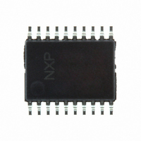
TDA1517ATW/N1,112 NXP Semiconductors, TDA1517ATW/N1,112 Datasheet - Page 7

TDA1517ATW/N1,112
Manufacturer Part Number
TDA1517ATW/N1,112
Description
IC AMP AUDIO PWR 8W STER 20TSSOP
Manufacturer
NXP Semiconductors
Type
Class Br
Datasheet
1.TDA1517ATWN1118.pdf
(19 pages)
Specifications of TDA1517ATW/N1,112
Output Type
1-Channel (Mono) or 2-Channel (Stereo)
Package / Case
20-TSSOP Exposed Pad, 20-eTSSOP, 20-HTSSOP
Max Output Power X Channels @ Load
8W x 1 @ 8 Ohm; 4W x 2 @ 4 Ohm
Voltage - Supply
6 V ~ 18 V
Features
Depop, Mute, Short-Circuit and Thermal Protection, Standby
Mounting Type
Surface Mount
Product
Class-AB
Output Power
8 W
Available Set Gain
26 dB
Thd Plus Noise
0.03 %
Operating Supply Voltage
12 V
Supply Current
40 mA
Maximum Power Dissipation
5 W
Maximum Operating Temperature
+ 85 C
Mounting Style
SMD/SMT
Audio Load Resistance
8 Ohms
Input Signal Type
Differential
Minimum Operating Temperature
- 40 C
Output Signal Type
Differential, Single
Supply Type
Single
Supply Voltage (max)
18 V
Supply Voltage (min)
6 V
Operational Class
Class-AB
Output Power (typ)
8x1@8Ohm/4x2@4OhmW
Audio Amplifier Function
Speaker
Total Harmonic Distortion
0.03@8Ohm@1W%
Single Supply Voltage (typ)
12V
Dual Supply Voltage (typ)
Not RequiredV
Power Supply Requirement
Single
Power Dissipation
5W
Rail/rail I/o Type
No
Single Supply Voltage (min)
6V
Single Supply Voltage (max)
18V
Dual Supply Voltage (min)
Not RequiredV
Dual Supply Voltage (max)
Not RequiredV
Operating Temp Range
-40C to 85C
Operating Temperature Classification
Industrial
Mounting
Surface Mount
Pin Count
20
Lead Free Status / RoHS Status
Lead free / RoHS Compliant
Lead Free Status / RoHS Status
Lead free / RoHS Compliant, Lead free / RoHS Compliant
Other names
568-3500-5
935268373112
TDA1517ATWDH
935268373112
TDA1517ATWDH
NXP Semiconductors
Notes to the characteristics
1. R
2. Output power is measured directly at the output pins of the IC.
3. Frequency response externally fixed.
4. V
5. Noise voltage measured in a bandwidth of 20 Hz to 20 kHz.
6. Noise output voltage independent of R
7. V
8. R
APPLICATION INFORMATION
2001 Apr 17
handbook, full pagewidth
8 W BTL or 2 × 4 W SE power amplifier
ripple
i
L
L
= V
= 4 Ω, measured in Fig.4.
= 8 Ω, measured in Fig.3.
i(max)
= V
ripple(max)
On
Mute
Standby
CONTROLLER
= 1 V (RMS).
MICRO-
μc1
0
0
1
= 2 V (p-p); R
μc1
μc2
μc2
0
1
0
+IN1
10 kΩ
V CC
470 nF
S
8.2
kΩ
= 0 Ω.
MODE
Fig.3 BTL application block diagram.
S
.
18
17
3
5
15 kΩ
TDA1517ATW
15 kΩ
MUTE LOGIC
STANDBY/
60 kΩ
60 kΩ
R i
R i
7
reference
voltage
input
V CC
SGND
15
4
SHORT CIRCUIT
TEMPERATURE
PROTECTION
A
B
10
AND
16
PGND
11
12
13
8
9
100
nF
+OUT
−OUT
MGU304
TDA1517ATW
Product specification
1000
μF
R L
8 Ω
V CC


