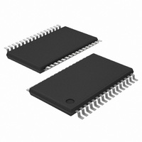
TDA8932BTW/N2,112 NXP Semiconductors, TDA8932BTW/N2,112 Datasheet - Page 26

TDA8932BTW/N2,112
Manufacturer Part Number
TDA8932BTW/N2,112
Description
IC AMP AUDIO 55W STER D 32TSSOP
Manufacturer
NXP Semiconductors
Type
Class Dr
Datasheet
1.TDA8932BTWN2118.pdf
(48 pages)
Specifications of TDA8932BTW/N2,112
Package / Case
32-TSSOP Exposed Pad, 32-eTSSOP, 32-HTSSOP
Output Type
1-Channel (Mono) or 2-Channel (Stereo)
Max Output Power X Channels @ Load
55W x 1 @ 8 Ohm; 26.5W x 2 @ 4 Ohm
Voltage - Supply
10 V ~ 36 V, ±5 V ~ 18 V
Features
Depop, Differential Inputs, Mute, Short-Circuit and Thermal Protection
Mounting Type
Surface Mount
Mounting Style
SMD/SMT
Lead Free Status / RoHS Status
Lead free / RoHS Compliant
Other names
935283479112
TDA8932BTW
TDA8932BTW
TDA8932BTW/N2
TDA8932BTW/N2
TDA8932BTW
TDA8932BTW
TDA8932BTW/N2
TDA8932BTW/N2
NXP Semiconductors
TDA8932B_4
Product data sheet
14.6 Device synchronization
14.7 Thermal behavior (printed-circuit board considerations)
Where:
Example:
Substituting R1 = R2 = 4.7 k , Z
results in a gain of G
If two or more TDA8932B devices are used in one application it is recommended that all
devices are synchronized running at the same switching frequency to avoid beat tones.
Synchronization can be realized by connecting all OSCIO pins together and configuring
one of the TDA8932B devices as master, while the other TDA8932B devices are
configured as slaves (see
A device is configured as master when connecting a resistor between pins OSCREF and
V
oscillator output for synchronization. The OSCREF pins of the slave devices should be
shorted to V
The TDA8932B is available in two different thermally enhanced packages:
The SO32 package has special thermal corner-leads, increasing the power capability
(reducing the overall R
and 32) should be attached to a copper plane. The SO32 package is very suitable for
applications with limited space for a thermal plane (in a single layer PCB design).
R
Fig 11. Master slave concept in two chip application
SSD(HW)
EQ
R
R3 = parallel resistor ( )
Z
TDA8932BT in a SO32 (SOT287-1) package for reflow and wave solder process
TDA8932BTW in an HTSSOP32 (SOT549-1) package for reflow solder process only
i
EQ
= internal input impedance ( )
=
= equivalent resistance ( )
----------------- -
R3
R3
setting the carrier frequency. Pin OSCIO of the master is then configured as an
+
SSD(HW)
Z
Z
i
i
100 nF
C osc
configuring pin OSCIO as an input.
master
v(tot)
Rev. 04 — 18 December 2008
OSCREF V
th(j-a)
= 26.3 dB.
Figure
R osc
39 k
. To benefit from the corner leads pins V
TDA8932B
SSD(HW)
IC1
i
11).
= 100 k and R3 = 22 k in
OSCIO
slave
OSCIO
TDA8932B
V
SSD(HW)
IC2
Equation 8
Class-D audio amplifier
OSCREF
SSD(HW)
001aaf600
TDA8932B
© NXP B.V. 2008. All rights reserved.
and
(pins 1, 16, 17
Equation 9
26 of 48
(9)


