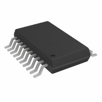
AD8331ARQ-REEL Analog Devices Inc, AD8331ARQ-REEL Datasheet - Page 27

AD8331ARQ-REEL
Manufacturer Part Number
AD8331ARQ-REEL
Description
IC VGA SINGLE W/PREAMP 20-SSOP
Manufacturer
Analog Devices Inc
Series
X-AMP®r
Type
Variable Gain Amplifierr
Datasheet
1.AD8331ARQZ.pdf
(56 pages)
Specifications of AD8331ARQ-REEL
Rohs Status
RoHS non-compliant
Design Resources
Interfacing the High Frequency AD8331 to AD9215 (CN0096)
Applications
Signal Processing
Mounting Type
Surface Mount
Package / Case
20-QSOP
For Use With
AD8331-EVALZ - BOARD EVAL FOR AD8331
The primary purpose of input impedance matching is to
improve the system transient response. With resistive termination,
the input noise increases due to the thermal noise of the matching
resistor and the increased contribution of the LNA input voltage
noise generator. With active impedance matching, however, the
contributions of both are smaller than they would be for resistive
termination by a factor of 1/(1 + LNA Gain). Figure 76 shows
their relative NF performance. In this graph, the input impedance
is swept with R
figures for a source impedance of 50 Ω are 7.1 dB, 4.1 dB, and
2.5 dB, respectively, for the resistive, active, and unterminated
configurations. The noise figures for 200 Ω are 4.6 dB, 2.0 dB,
and 1.0 dB, respectively.
Figure 77 is a plot of NF vs. R
helpful for design purposes. The plateau in the NF for actively
matched inputs mitigates source impedance variations. For
comparison purposes, a preamp with a gain of 19 dB and noise
spectral density of 1.0 nV/√Hz, combined with a VGA with
3.75 nV/√Hz, yields a noise figure degradation of approximately
1.5 dB (for most input impedances), significantly worse than
the
The equivalent input noise of the LNA is the same for single-
ended and differential output applications. The LNA noise figure
improves to 3.5 dB at 50 Ω without VGA noise, but this is
exclusive of noise contributions from other external circuits
connected to LOP. A series output resistor is usually recom-
mended for stability purposes when driving external circuits on
a separate board (see the Applications Information section). In
low noise applications, a ferrite bead is even more desirable.
VARIABLE GAIN AMPLIFIER
The differential X-AMP VGA provides precise input attenuation
and interpolation. It has a low input-referred noise of 2.7 nV/√Hz
and excellent gain linearity. A simplified block diagram is shown
in Figure 78.
200Ω
GAIN
AD8331/AD8332/AD8334
VIN
VIP
g
m
6dB
R
S
GAIN INTERPOLATOR
to preserve the match at each point. The noise
(BOTH CHANNELS)
Figure 78. Simplified VGA Schematic
2R
S
for various values of R
performance.
48dB
+
–
POSTAMP
POSTAMP
IN
, which is
Rev. G | Page 27 of 56
X-AMP VGA
The input of the VGA is a differential R-2R ladder attenuator
network with 6 dB steps per stage and a net input impedance of
200 Ω differential. The ladder is driven by a fully differential
input signal from the LNA and is not intended for single-ended
operation. LNA outputs are ac-coupled to reduce offset and isolate
their common-mode voltage. The VGA inputs are biased through
the center tap connection of the ladder to VCM, which is typically
set to 2.5 V and is bypassed externally to provide a clean ac ground.
The signal level at successive stages in the input attenuator
falls from 0 dB to −48 dB in +6 dB steps. The input stages of the
X-AMP are distributed along the ladder, and a biasing interpolator,
controlled by the gain interface, determines the input tap point.
With overlapping bias currents, signals from successive taps
merge to provide a smooth attenuation range from 0 dB to
−48 dB. This circuit technique results in excellent linear-in-dB
gain law conformance and low distortion levels and deviates
±0.2 dB or less from the ideal. The gain slope is monotonic with
respect to the control voltage and is stable with variations in
process, temperature, and supply.
The X-AMP inputs are part of a gain-of-12 feedback amplifier
that completes the VGA. Its bandwidth is 150 MHz. The input
stage is designed to reduce feedthrough to the output and to
ensure excellent frequency response uniformity across gain
setting (see Figure 12 and Figure 13).
Gain Control
Position along the VGA attenuator is controlled by a single-ended
analog control voltage, V
1.0 V. The gain control scaling is trimmed to a slope of 50 dB/V
(20 mV/dB). Values of V
to minimum or maximum gain values. Both channels of the
AD8332 are controlled from a single gain interface to preserve
matching. Gain can be calculated using Equation 1 and Equation 2.
Gain accuracy is very good because both the scaling factor and
absolute gain are factory trimmed. The overall accuracy relative
to the theoretical gain expression is ±1 dB for variations in
temperature, process, supply voltage, interpolator gain ripple,
trim errors, and tester limits. The gain error relative to a best-fit
line for a given set of conditions is typically ±0.2 dB. Gain matching
between channels is better than 0.1 dB (Figure 11 shows gain errors
in the center of the control range). When V
gain errors are slightly greater.
The gain slope can be inverted, as shown in Figure 73 (except for
the AD8332 AR models). The gain drops with a slope of −50 dB/V
across the gain control range from maximum to minimum gain.
This slope is useful in applications such as automatic gain control,
where the control voltage is proportional to the measured output
signal amplitude. The inverse gain mode is selected by setting the
MODE pin to HI gain mode.
Gain control response time is less than 750 ns to settle within 10%
of the final value for a change from minimum to maximum gain.
GAIN
AD8331/AD8332/AD8334
GAIN
, with an input range of 40 mV to
beyond the control range saturate
GAIN
< 0.1 or > 0.95,


