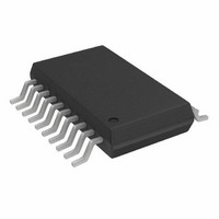
AD8331ARQ-REEL Analog Devices Inc, AD8331ARQ-REEL Datasheet - Page 30

AD8331ARQ-REEL
Manufacturer Part Number
AD8331ARQ-REEL
Description
IC VGA SINGLE W/PREAMP 20-SSOP
Manufacturer
Analog Devices Inc
Series
X-AMP®r
Type
Variable Gain Amplifierr
Datasheet
1.AD8331ARQZ.pdf
(56 pages)
Specifications of AD8331ARQ-REEL
Rohs Status
RoHS non-compliant
Design Resources
Interfacing the High Frequency AD8331 to AD9215 (CN0096)
Applications
Signal Processing
Mounting Type
Surface Mount
Package / Case
20-QSOP
For Use With
AD8331-EVALZ - BOARD EVAL FOR AD8331
AD8331/AD8332/AD8334
APPLICATIONS INFORMATION
LNA—EXTERNAL COMPONENTS
The LMD pin (connected to the bias circuitry) must be bypassed to
ground and signal sourced to the INH pin, which is capacitively
coupled using 2.2 nF to 0.1 μF capacitors (see Figure 81).
The unterminated input impedance of the LNA is 6 kΩ. The
user can synthesize any LNA input resistance between 50 Ω and
6 kΩ. R
Table 7.
Table 7. LNA External Component Values for Common
Source Impedances
R
50
75
100
200
500
6 k
When active input termination is used, a decoupling capacitor (C
is required to isolate the input and output bias voltages of the LNA.
The shunt input capacitor, C
frequencies where the active termination match is lost due to
the gain roll-off of the LNA at high frequencies. The value of C
diminishes as R
required. Suggested values for C
shown in Table 7.
When a long trace to Pin INH is unavoidable, or if both LNA
outputs drive external circuits, a small ferrite bead (FB) in series
with Pin INH preserves circuit stability with negligible effect on
noise. The bead shown is 75 Ω at 100 MHz (Murata BLM21 or
equivalent). Other values can prove useful.
Figure 82 shows the interconnection details of the LNA output.
Capacitive coupling between the LNA outputs and the VGA
inputs is required because of the differences in their dc levels
and the need to eliminate the offset of the LNA. Capacitor values
of 0.1 μF are recommended. There is a 0.4 dB loss in gain
between the LNA output and the VGA input due to the 5 Ω
output resistance. Additional loading at the LOP and LON
outputs affects LNA gain.
IN
(Ω)
R
IZ
IZ
=
is calculated according to Equation 6 or selected from
33
6
R
280
412
562
1.13 k
3.01 k
∞
kΩ
IZ
kΩ
(Nearest STD 1% Value, Ω)
IN
–
increases to 500 Ω, at which point no capacitor is
×
( )
R
( )
R
IN
IN
SH
, reduces gain peaking at higher
SH
for 50 Ω ≤ R
IN
≤ 200 Ω are
C
22
12
8
1.2
None
None
SH
(pF)
SH
Rev. G | Page 30 of 56
(6)
IS
)
V
Both LNA outputs are available for driving external circuits.
Pin LOP should be used in those instances when a single-ended
LNA output is required. The user should be aware of stray
capacitance loading of the LNA outputs, in particular LON. The
LNA can drive 100 Ω in parallel with 10 pF. If an LNA output is
routed to a remote PC board, it tolerates a load capacitance up
to 100 pF with the addition of a 49.9 Ω series resistor or ferrite
75 Ω/100 MHz bead.
0.1µF
GAIN
0.1µF
Figure 81. Basic Connections for a Typical Channel
1nF
C
1nF
1nF
SH
Figure 82. Interconnections of the LNA and VGA
+5V
10
11
12
13
14
3.25V
1
2
3
4
5
6
7
8
9
3.25V
LMD2
INH2
VPS2
LON2
LOP2
COM2
VIP2
VIN2
VCM2
GAIN
RCLMP
VOH2
VOL2
COMM
LNA
*SEE TEXT
C
0.1µF
LMD
2.5V
2.5V
COM1
LMD1
VCM1
VOH1
LON1
LOP1
VOL1
VPSV
VPS1
HILO
5Ω
5Ω
INH1
VIP1
VIN1
ENB
R
IZ
28
27
26
25
24
23
22
21
20
19
18
17
16
15
1nF
LOP
LON
DECOUPLING
DECOUPLING
5V
*
*
RESISTOR
RESISTOR
5V
0.1µF
R
1nF
LNA
LNA
C
IZ
IZ
*
*
VGA OUT
VGA OUT
FB
1nF
VCM
VIP
VIN
LNA OUT
C
(AD8332
0.1µF
SH
5V
*
0.1µF
50Ω
50Ω
Shown)
5V
0.1µF
0.1µF
CIRCUIT
CIRCUIT
TO EXT
100Ω
100Ω
TO EXT
SOURCE
LNA


