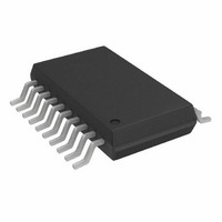
AD8331ARQ-REEL Analog Devices Inc, AD8331ARQ-REEL Datasheet - Page 31

AD8331ARQ-REEL
Manufacturer Part Number
AD8331ARQ-REEL
Description
IC VGA SINGLE W/PREAMP 20-SSOP
Manufacturer
Analog Devices Inc
Series
X-AMP®r
Type
Variable Gain Amplifierr
Datasheet
1.AD8331ARQZ.pdf
(56 pages)
Specifications of AD8331ARQ-REEL
Rohs Status
RoHS non-compliant
Design Resources
Interfacing the High Frequency AD8331 to AD9215 (CN0096)
Applications
Signal Processing
Mounting Type
Surface Mount
Package / Case
20-QSOP
For Use With
AD8331-EVALZ - BOARD EVAL FOR AD8331
Gain Input
The GAIN pin is common to both channels of the AD8332. The
input impedance is nominally 10 MΩ, and a bypass capacitor
from 100 pF to 1 nF is recommended.
Parallel connected devices can be driven by a common voltage
source or DAC. Decoupling should take into account any band-
width considerations of the drive waveform, using the total
distributed capacitance.
If gain control noise in LO gain mode becomes a factor, main-
taining ≤15 nV/√Hz noise at the GAIN pin ensures satisfactory
noise performance. Internal noise prevails below 15 nV/√Hz at
the GAIN pin. Gain control noise is negligible in HI gain mode.
VCM Input
The common-mode voltage of Pin VCM, Pin VOL, and Pin VOH
defaults to 2.5 V dc. With output ac-coupled applications, the
VCM pin is unterminated; however, it must still be bypassed in
close proximity for ac grounding of internal circuitry. The VGA
outputs can be dc connected to a differential load, such as an
ADC. Common-mode output voltage levels between 1.5 V and
3.5 V can be realized at Pin VOH and Pin VOL by applying the
desired voltage at Pin VCM. DC-coupled operation is not
recommended when driving loads on a separate PC board.
The voltage on the VCM pin is sourced by an internal buffer
with an output impedance of 30 Ω and a ±2 mA default output
current (see Figure 83). If the VCM pin is driven from an external
source, its output impedance should be <<30 Ω, and its current
drive capability should be >>2 mA. If the VCM pins of several
devices are connected in parallel, the external buffer should be
capable of overcoming their collective output currents. When a
common-mode voltage other than 2.5 V is used, a voltage-
limiting resistor, R
Logic Inputs—ENB, MODE, and HILO
The input impedance of all enable pins is nominally 25 kΩ and
can be pulled up to 5 V (a pull-up resistor is recommended) or
driven by any 3 V or 5 V logic families. The enable pin, ENB,
powers down the VGA; when pulled low, the VGA output voltages
are near ground. Multiple devices can be driven from a common
source. Consult Table 3, Table 4, Table 5, and Table 6 for infor-
mation about circuit functions controlled by the enable pins.
Pin HILO is compatible with 3 V or 5 V CMOS logic families. It
is either connected to ground or pulled up to 5 V, depending on
the desired gain range and output noise.
2mA MAX
AC GROUNDING FOR
INTERNAL CIRCUITRY
CLMP
30Ω
Figure 83. VCM Interface
CIRCUITRY
, is needed to protect against overload.
INTERNAL
100pF
VCM
R
O
<< 30Ω
0.1µF
NEW V
CM
Rev. G | Page 31 of 56
Optional Output Voltage Limiting
The RCLMP pin provides the user with a means to limit the
output voltage swing when used with loads that have no
provisions for prevention of input overdrive. The peak-to-peak
limited voltage is adjusted by a resistor to ground (see Table 8
for a list of several voltage levels and corresponding resistor
values). Unconnected, the default limiting level is 4.5 V p-p.
Note that third harmonic distortion increases as waveform
amplitudes approach clipping. For lowest distortion, the clamp level
should be set higher than the converter input span. A clamp level
of 1.5 V p-p is recommended for a 1 V p-p linear output range,
2.7 V p-p for a 2 V p-p range, or 1 V p-p for a 0.5 V p-p operation.
The best solution is determined experimentally. Figure 84 shows
third harmonic distortion as a function of the limiting level for
a 2 V p-p output signal. A wider limiting level is desirable in HI
gain mode.
Table 8. Clamp Resistor Values
Clamp Level (V p-p)
0.5
1.0
1.5
2.0
2.5
3.0
3.5
4.0
4.4
Output Decoupling
When driving capacitive loads greater than about 10 pF, or long
circuit connections on other boards, an output network of resistors
and/or ferrite beads can be useful to ensure stability. These
components can be incorporated into a Nyquist filter such as
the one shown in Figure 81. In Figure 81, the resistor value is
84.5 Ω. For example, all the evaluation boards for this series
incorporate 100 Ω in parallel with a 120 nH bead. Lower value
resistors are permissible for applications with nearby loads or
Figure 84. HD3 vs. Clamping Level for 2 V p-p Differential Input
–20
–30
–40
–50
–60
–70
–80
1.5
V
GAIN
2.0
= 0.75V
2.5
CLAMP LIMIT LEVEL (V p-p)
AD8331/AD8332/AD8334
HILO = LO
1.21
2.74
4.75
7.5
11
16.9
26.7
49.9
100
3.0
Clamp Resistor Value (kΩ)
HILO = LO
HILO = HI
3.5
4.0
HILO = HI
2.21
4.02
6.49
9.53
14.7
23.2
39.2
73.2
4.5
5.0


