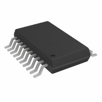
AD8331ARQ-REEL Analog Devices Inc, AD8331ARQ-REEL Datasheet - Page 33

AD8331ARQ-REEL
Manufacturer Part Number
AD8331ARQ-REEL
Description
IC VGA SINGLE W/PREAMP 20-SSOP
Manufacturer
Analog Devices Inc
Series
X-AMP®r
Type
Variable Gain Amplifierr
Datasheet
1.AD8331ARQZ.pdf
(56 pages)
Specifications of AD8331ARQ-REEL
Rohs Status
RoHS non-compliant
Design Resources
Interfacing the High Frequency AD8331 to AD9215 (CN0096)
Applications
Signal Processing
Mounting Type
Surface Mount
Package / Case
20-QSOP
For Use With
AD8331-EVALZ - BOARD EVAL FOR AD8331
When selecting overload protection, the important parameters
are forward and reverse voltages and t
BAS40-04 series shown in Figure 88 has a τ
of 310 mV at 1 mA. Many variations of these specifications can
be found in vendor catalogs.
LAYOUT, GROUNDING, AND BYPASSING
Due to their excellent high frequency characteristics, these
devices are sensitive to their PCB environments. Realizing
expected performance requires attention to detail critical to
good, high speed, board design.
A multilayer board with power and ground planes is recom-
mended with blank areas in the signal layers filled with ground
plane. Be certain that the power and ground pins provided for
robust power distribution to the device are connected. Decouple
the power supply pins with surface-mount capacitors as close as
possible to each pin to minimize impedance paths to ground.
Decouple the LNA power pins from the VGA supply using
ferrite beads. Together with the capacitors, ferrite beads
eliminate undesired high frequencies without reducing the
headroom. Use a larger value capacitor for every 10 chips to
20 chips to decouple residual low frequency noise. To minimize
voltage drops, use a 5 V regulator for the VGA array.
Several critical LNA areas require special care. The LON and
LOP output traces must be as short as possible before connecting
to the coupling capacitors connected to Pin VIN and Pin VIP.
R
placed as close as possible to the VGA output pins, VOL and
VOH, to mitigate loading effects of connecting traces. Values
are discussed in the Output Decoupling section.
Signal traces must be short and direct to avoid parasitic effects.
Wherever there are complementary signals, symmetrical layout
should be employed to maintain waveform balance. PCB traces
should be kept adjacent when running differential signals over a
long distance.
MULTIPLE INPUT MATCHING
Matching of multiple sources with dissimilar impedances can be
accomplished as shown in Figure 89. A relay and low supply voltage
analog switch can be used to select between multiple sources
and their associated feedback resistors. An
switch is shown in this example; however, multiple switches are
also available and users are referred to the
Selection Guide
IZ
must be placed near the LON pin as well. Resistors must be
for switches and multiplexers.
rr
(or τ
Analog Devices
ADG736
rr
rr
of 100 ps and a V
). The Infineon
dual SPDT
Rev. G | Page 33 of 56
F
DISABLING THE LNA
Where accessible, connection of the LNA enable pin to ground
powers down the LNA, resulting in a current reduction of about
half. In this mode, the LNA input and output pins can be left
unconnected; however, the power must be connected to all the
supply pins for the disabling circuit to function. Figure 90 illustrates
the connections using
+5V
200Ω
50Ω
MODE
GAIN
0.1µF
VIN
0.1µF
Figure 89. Accommodating Multiple Sources
NC
NC
NC
NC
10
0.1µF
1
2
3
4
5
6
7
8
9
Figure 90. Disabling the LNA
18nF
LMD
INH
VPSL
LON
LOP
COML
VIP
VIN
MODE
GAIN
AD8331
AD8331/AD8332/AD8334
AD8331
SELECT R
AD8332
LMD
INH
as an example.
RCLMP
COMM
COMM
ENBV
VPOS
ENBL
HILO
VCM
VOH
VOL
ADG736
IZ
20
19
18
17
16
15
14
13
12
11
LNA
VOUT
1.13kΩ
280Ω
+5V
5Ω
HILO
5Ω
VCM
LON
LOP
R
+5V
CLMP


