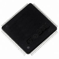
TDA7500A STMicroelectronics, TDA7500A Datasheet - Page 3

TDA7500A
Manufacturer Part Number
TDA7500A
Description
IC PROCESSOR AM/FM DGTL 100-TQFP
Manufacturer
STMicroelectronics
Type
Audio Processorr
Datasheet
1.TDA7500ATR.pdf
(40 pages)
Specifications of TDA7500A
Applications
Audio Systems
Mounting Type
Surface Mount
Package / Case
100-TQFP Exposed Pad, 100-eTQFP, 100-HTQFP, 100-VQFP
Lead Free Status / RoHS Status
Lead free / RoHS Compliant
Available stocks
Company
Part Number
Manufacturer
Quantity
Price
Company:
Part Number:
TDA7500ATR
Manufacturer:
STMicroelectronics
Quantity:
10 000
Part Number:
TDA7500ATR
Manufacturer:
ST
Quantity:
20 000
PIN DESCRIPTION
N°
10
11
12
13
1
2
3
4
5
6
7
8
9
GND1
VDD1
TESTEN
TESTSE
NRESET
SCKM/DSP0_GPIO0
MISOM/DSP0_GPIO1
MOSIM/DSP0_GPIO2
SSM/DSP0_GPIO3
SCKD/DSP0_GPIO4
MISOD/DSP0_GPIO5
MISOD/DSP0_GPIO6
SSD/DSP0_GPIO7
Name
Type
I/O
I/O
I/O
I/O
I/O
I
I
I
I
I
I
Ground pin dedicated to the digital circuitry.
Supply pin dedicated to the digital circuitry.
muxes the XTI clock to all flip-flops. When TEST_SE is also
active, the scan chain shifting is enabled. To be connected to
Vdd in operating mode.
controls the shifting of the internal scan chains. When active with
TESTEN not active, sets all tri-state outputs into hi-impedance
mode. To be connected to GND in operating mode.
System Reset (Input). A low level applied to NRESET input
initializes the IC.
I
General Purpose I/O (Input/Output). Clock line for I
interface is enabled, behaves as SPI bit clock. Optionally it can
be used as general purpose I/O controlled by DSP0.
I
Output Serial Data (Input/Output)/General Purpose I/O (Input/
Output). Data line for I
Serial Data Input when in SPI Master Mode and Serial Data
Output when in SPI Slave Mode. Optionally it can be used as
general purpose I/O controlled by DSP0.
General Purpose I/O (Input/Output). Serial Data Output when in
SPI Master Mode and Serial Data Input when in SPI Slave
Mode. Optionally it can be used as general purpose I/O
controlled by DSP0.
SPI is enabled, behaves as Slave Select line for SPI bus.
Optionally it can be used as general purpose I/O controlled by
DSP0.
clock. Optionally it can be used as general purpose I/O
controlled by DSP0.
General Purpose I/O (Input/Output). Behaves as Serial Data
Input when in SPI Master Mode and Serial Data Output when in
SPI Slave Mode. Optionally it can be used as general purpose I/
O controlled by DSP0.
General Purpose I/O (Input/Output). Serial Data Output when in
SPI Master Mode and Serial Data Input when in SPI Slave
Mode. Optionally it can be used as general purpose I/O
controlled by DSP0.
Behaves as Slave Select line for SPI bus. Optionally it can be
used as general purpose I/O controlled by DSP0.
Test Enable (Input). When low, puts the chip into test mode and
SCAN Enable (Input). When high with TESTEN also active,
SPI Master Output Slave Input Serial Data (Input/Output)/
SPI Slave Select (Input)/General Purpose I/O (Input/Output). If
SPI Bit Clock (Input)/General Purpose I/O (Input/Output). SPI bit
SPI Master Input Slave Output Serial Data (Input/Output)/
SPI Master Output Slave Input Serial Data (Input/Output)/
SPI Slave Select (Input)/General Purpose I/O (Input/Output).
2
2
C Serial Clock Line (Input/Output)/SPI Bit Clock (Input)/
C Serial Data Line (Input/Output)/SPI Master Input Slave
2
C bus. If SPI is enabled, behaves as
Description
2
TDA7500A
C bus. If SPI
3/40


