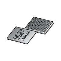
LPC1850FET256 NXP Semiconductors, LPC1850FET256 Datasheet - Page 62

LPC1850FET256
Manufacturer Part Number
LPC1850FET256
Description
The LPC1850FET256 is a high-performance, cost-effective Cortex-M3 microcontroller featuring 200 kB of SRAM, and advanced peripherals including Ethernet, High Speed USB 2
Manufacturer
NXP Semiconductors
Datasheet
1.LPC1810FBD144.pdf
(157 pages)
Available stocks
Company
Part Number
Manufacturer
Quantity
Price
Company:
Part Number:
LPC1850FET256
Manufacturer:
NXP
Quantity:
1 000
Part Number:
LPC1850FET256
Manufacturer:
NXP/恩智浦
Quantity:
20 000
Company:
Part Number:
LPC1850FET256,551
Manufacturer:
NXP Semiconductors
Quantity:
10 000
Part Number:
LPC1850FET256,551
Manufacturer:
NXP/恩智浦
Quantity:
20 000
NXP Semiconductors
Table 3.
LCD, Ethernet, USB0, and USB1 functions are not available on all parts. See
LPC1850_30_20_10
Preliminary data sheet
Symbol
CLK2
CLK3
Debug pins
DBGEN
TCK/SWDCLK
TRST
TMS/SWDIO
TDO/SWO
TDI
USB0 pins
USB0_DP
USB0_DM
USB0_VBUS
Pin description
D14
P12
L4
J5
M4
K6
K5
J4
F2
G2
F1
x
x
x
x
x
x
x
x
x
x
x
…continued
K6
-
A6
H2
B4
C4
H3
G3
E1
E2
E3
38
141 99
-
41
42
44
46
35
26
28
29
All information provided in this document is subject to legal disclaimers.
-
28
27
29
30
31
26
18
20
21
Rev. 3.1 — 15 December 2011
68
-
18
17
19
20
21
16
9
11
12
[5]
[5]
[3]
[3]
[3]
[3]
[3]
[3]
[7]
[7]
[7]
[8]
O;
PU
O;
PU
I
I; F
I; PU I
I; PU I
O
I; PU I
-
-
-
O
O
-
-
I/O SD_CLK — SD/MMC card clock.
O
O
I/O I2S1_RX_SCK — Receive Clock. It is driven by the
O
O
-
-
-
O
-
I/O I2S1_RX_SCK — Receive Clock. It is driven by the
I
I
O
I/O USB0 bidirectional D+ line.
I/O USB0 bidirectional D line.
I/O VBUS pin (power on USB cable). This pin includes
Description
EMC_CLK3 — SDRAM clock 3.
CLKOUT — Clock output pin.
R — Function reserved.
R — Function reserved.
EMC_CLK23 — SDRAM clock 2 and clock 3
combined.
I2S0_TX_MCLK — I
master and received by the slave. Corresponds to
the signal SCK in the I
EMC_CLK2 — SDRAM clock 2.
CLKOUT — Clock output pin.
R — Function reserved.
R — Function reserved.
R — Function reserved.
CGU_OUT1 — CGU spare clock output 1.
R — Function reserved.
master and received by the slave. Corresponds to
the signal SCK in the I
JTAG interface control signal. Also used for boundary
scan.
Test Clock for JTAG interface (default) or Serial Wire
(SW) clock.
Test Reset for JTAG interface.
Test Mode Select for JTAG interface (default) or SW
debug data input/output.
Test Data Out for JTAG interface (default) or SW
trace output.
Test Data In for JTAG interface.
an internal pull-down resistor of 64 k (typical)
16 k.
Table
32-bit ARM Cortex-M3 microcontroller
LPC1850/30/20/10
2.
2
S transmit master clock.
2
2
S-bus specification.
S-bus specification.
© NXP B.V. 2011. All rights reserved.
62 of 157


