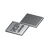
LPC1850FET256 NXP Semiconductors, LPC1850FET256 Datasheet - Page 87

LPC1850FET256
Manufacturer Part Number
LPC1850FET256
Description
The LPC1850FET256 is a high-performance, cost-effective Cortex-M3 microcontroller featuring 200 kB of SRAM, and advanced peripherals including Ethernet, High Speed USB 2
Manufacturer
NXP Semiconductors
Datasheet
1.LPC1810FBD144.pdf
(157 pages)
Available stocks
Company
Part Number
Manufacturer
Quantity
Price
Company:
Part Number:
LPC1850FET256
Manufacturer:
NXP
Quantity:
1 000
Part Number:
LPC1850FET256
Manufacturer:
NXP/恩智浦
Quantity:
20 000
Company:
Part Number:
LPC1850FET256,551
Manufacturer:
NXP Semiconductors
Quantity:
10 000
Part Number:
LPC1850FET256,551
Manufacturer:
NXP/恩智浦
Quantity:
20 000
NXP Semiconductors
LPC1850_30_20_10
Preliminary data sheet
7.18.2 System Control Unit (SCU)
7.18.3 Clock Generation Unit (CGU)
7.18.4 Internal RC oscillator (IRC)
7.18.5 PLL0USB (for USB0)
7.18.6 PLL0AUDIO (for audio)
In addition, the CREG block contains the part identification and part configuration
information.
The system control unit determines the function and electrical mode of the digital pins. By
default function 0 is selected for all pins with pull-up enabled.
Analog I/Os for the ADCs and the DAC as well as most USB pins are on separate pads
and are not controlled through the SCU.
The Clock Generator Unit (CGU) generates several base clocks. The base clocks can be
unrelated in frequency and phase and can have different clock sources within the CGU.
One CGU base clock is routed to the CLKOUT pins. The base clock that generates the
CPU clock is referred to as CCLK.
Multiple branch clocks are derived from each base clock. The branch clocks offer very
flexible control for power-management purposes. All branch clocks are outputs of one of
two Clock Control Units (CCUs) and can be controlled independently. Branch clocks
derived from the same base clock are synchronous in frequency and phase.
The IRC is used as the clock source for the WWDT and/or as the clock that drives the
PLLs and subsequently the CPU. The nominal IRC frequency is 12 MHz. The IRC is
trimmed to 1 % accuracy over the entire voltage and temperature range.
Upon power-up or any chip reset, the LPC1850/30/20/10 use the IRC as the clock source.
Software may later switch to one of the other available clock sources.
PLL0 is a dedicated PLL for the USB0 High-speed controller.
PLL0 accepts an input clock frequency from an external oscillator in the range of 14 kHz
to 25 MHz. The input frequency is multiplied up to a high frequency with a Current
Controlled Oscillator (CCO). The CCO operates in the range of 4.3 MHz to 550 MHz.
The audio PLL PLL0AUDIO is a general purpose PLL with a very small step size. This
PLL accepts an input clock frequency derived from an external oscillator or internal IRC.
The input frequency is multiplied up to a high frequency with a Current Controlled
Oscillator (CCO). A sigma-delta converter modulates the PLL divider ratios to obtain the
desired output frequency. The output frequency can be set as a multiple of the sampling
frequency f
frequency f
Many other frequencies are possible as well.
•
•
Timer/USART inputs
Enabling the USB controllers
s
s
to 32f
can range from 16 kHz to 192 kHz (16, 22.05, 32, 44.1, 48, 96,192) kHz.
All information provided in this document is subject to legal disclaimers.
s
Rev. 3.1 — 15 December 2011
, 64f
s
, 128 f
s
, 256 f
s
, 384 f
32-bit ARM Cortex-M3 microcontroller
LPC1850/30/20/10
s
, 512 f
s
and the sampling
© NXP B.V. 2011. All rights reserved.
87 of 157


