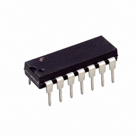
LM319N Fairchild Semiconductor, LM319N Datasheet - Page 3

LM319N
Manufacturer Part Number
LM319N
Description
IC COMPARATOR DUAL HS 14-DIP
Manufacturer
Fairchild Semiconductor
Type
General Purposer
Datasheet
1.LM319MX.pdf
(10 pages)
Specifications of LM319N
Number Of Elements
2
Output Type
DTL, Open-Collector, Open-Emitter, RTL, TTL
Voltage - Supply
5 V ~ 30 V, ±2.5 V ~ 15 V
Mounting Type
Through Hole
Package / Case
14-DIP (0.300", 7.62mm)
Number Of Channels
2 Channels
Response Time
80 ns
Offset Voltage (max)
8 mV
Input Bias Current (max)
1000 nA
Supply Voltage (max)
36 V
Supply Voltage (min)
+/- 15 V
Supply Current (max)
12.5 mA
Maximum Power Dissipation
500 mW
Maximum Operating Temperature
+ 70 C
Mounting Style
Through Hole
Minimum Operating Temperature
0 C
No. Of Comparators
2
Ic Output Type
Open Collector
Supply Voltage Range
5V To ± 15V
Amplifier Case Style
DIP
No. Of Pins
14
Operating Temperature Range
0°C To +70°C
Rohs Compliant
Yes
Comparator Type
High Speed
Supply Current
7.5mA
Lead Free Status / RoHS Status
Lead free / RoHS Compliant
Available stocks
Company
Part Number
Manufacturer
Quantity
Price
Part Number:
LM319N
Manufacturer:
NS/国半
Quantity:
20 000
Company:
Part Number:
LM319N/NOPB
Manufacturer:
TI
Quantity:
450
Electrical Characteristics
(V
Notes :
1. The offset voltage and offset currents given are the maximum values required to drive the output within a volt of either
2. The response time specified is for a 100mV input step with 5mV overdrive.
3. LM319 : 0
Input Offset Voltage (Note 1)
Input Offset Current (Note 1)
Input Bias Current
Voltage Gain
Response Time (Note 2)
Saturation Voltage
Output Leakage Current
Input Voltage Range
Differential Input Voltage
Positive Supply Current
Positive Supply Current
Negative Supply Current
CC
supply with a 1mA load. Thus, these parameters define an error band and take into account the worst case effects of
voltage gain and input impedance.
= + 15V, V
Parameter
T
A
EE
+70 C
= - 15V, T
A
Symbol
= 25 C, unless otherwise specified)
V
I
O(LKG)
T
I
V
V
I(DIFF)
I
I
BIAS
V
CC1
CC2
I
G
I
RES
SAT
I(R)
EE
IO
IO
V
R
V
V
V
V
V
V
Note 3
V
V
V
CC
CC
CC
I
I
I
CC
CC
CC
S
=15V, V
-10mV, I
5mV, V
10mV, V
= 15V
= 4.5V,V
= 5V, V
= 15V
= 15V
5K
O(P)
EE
EE
O
O(P)
EE
= -15V , V
= 0V
Conditions
= 35V
3.2mA
= 0V
= 35V
-
-
I
Note 3
Note 3
Note 3
Note3
Note 3
V
V
CC
CC
-5mV, I
= 15V
= 5V, V
O
= 25mA
EE
= 0V
Min. Typ. Max.
8
1
-
-
-
-
-
-
-
-
-
-
-
-
-
-
-
-
-
LM319
150 1000
2.0
0.6
0.3
0.2
3.6
7.5
10
40
80
13
3
-
-
-
-
-
-
-
1200
12.5
200
300
1.5
0.4
10
8.0
10
3
5
-
-
-
-
-
-
5
V/mV
LM319
Unit
mA
mV
mA
mA
nA
nA
ns
V
V
V
A
3


