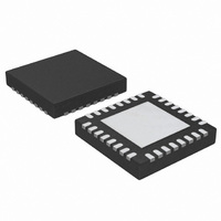
TDA8262HN/C1,118 NXP Semiconductors, TDA8262HN/C1,118 Datasheet - Page 21

TDA8262HN/C1,118
Manufacturer Part Number
TDA8262HN/C1,118
Description
IC SATELLITE TUNER 32-HVQFN
Manufacturer
NXP Semiconductors
Type
Satellite Tunerr
Datasheet
1.TDA8262HNC1118.pdf
(30 pages)
Specifications of TDA8262HN/C1,118
Package / Case
*
Applications
Demodulation
Mounting Type
Surface Mount
Bus Type
I2C
Maximum Agc
60 dB (Typ)
Maximum Frequency
2175 MHz
Minimum Frequency
950 MHz
Modulation Technique
QPSK
Mounting Style
SMD/SMT
Function
Satellite
Noise Figure
7.7 dB
Operating Supply Voltage
3.3 V
Supply Voltage (min)
3.15 V
Supply Voltage (max)
3.45 V
Minimum Operating Temperature
- 20 C
Maximum Operating Temperature
+ 85 C
Lead Free Status / RoHS Status
Lead free / RoHS Compliant
Lead Free Status / RoHS Status
Lead free / RoHS Compliant, Lead free / RoHS Compliant
Other names
935275321118
TDA8262HN/C1-T
TDA8262HN/C1-T
TDA8262HN/C1-T
TDA8262HN/C1-T
Philips Semiconductors
15. Characteristics
Table 39:
T
9397 750 13194
Product data sheet
Symbol
Supply
V
I
V
RF and Baseband
LO
Z
Z
Z
G
LO
RF
V
V
V
IIP
IIP
F
G
G
t
CC
d(g)(I-Q)
amb
i
o(l-t)i
L(I/Q)(max)
G
G
CC
POR
O(I/Q)
o(I/Q)(p-p)
o(I/Q)(rms)
LT
v(I-Q)(M)
v(I/Q)(R)
2
3
L(RFIN)
L(RFOUT)
isolation
v(BB)(min)
v(BB)(max)
= 25 C; V
Characteristics
Parameter
supply voltage
supply current
voltage limit when POR is active
LO leakage through RF inputs
input impedance
loop-through output impedance
maximum load on each IP, IN, QP
and QN output
LNA to loop-through gain
LO leakage on pin RFOUT
isolation between loop-through and
RF input
DC voltage on I/Q output
minimum baseband additional gain
maximum baseband additional gain BBGAIN [3:0] = Fh
typical AC output voltage on
differential I/Q output; peak-to-peak
value
recommended I and Q output
voltage RMS value (QPSK signals)
second-order interception point at
RF input
third-order interception point at RF
input
noise figure
voltage gain mismatch between I
and Q
voltage gain ripple for I or Q
absolute quadrature error
group delay mismatch in between I
and Q
CC
= 3.3 V; output level on differential I/Q output is 550 mV (p-p); unless otherwise specified.
Rev. 01 — 14 December 2004
Conditions
all power-down bits are 0
all power-down bits are 1
only bits PDXTOUT and PDXTAL
are 0
only bits PDLNA and PDLOOPT
are 0
between 950 MHz and 2175 MHz
single mode
LNA configuration
attenuated configuration
between 950 MHz and 2175 MHz
BBGAIN [3:0] = 0h
differential voltage
f
P
maximum gain; V
measured at 10 MHz;
f
f
measured at 10 MHz;
f
f
i
LPF
LPF
LPF
LPF
= 2150 MHz; P
RFIN
f
f
i
i
= 2150 MHz
= 950 MHz
= 36 MHz
= 36 MHz; 22.5 MHz band
= 36 MHz
= 36 MHz; 22.5 MHz band
= 20 dBm
RFIN
AGC
= 20 dBm
= 3 V
Fully integrated satellite tuner
[1]
[2]
[3]
© Koninklijke Philips Electronics N.V. 2004. All rights reserved.
Min
3.15
-
-
-
-
1.5
-
-
-
-
-
-
-
-
-
-
-
-
-
-
-
-
-
-
-
0
-
2
TDA8262HN
Typ
3.3
175
6
30
45
-
75
75
10
1
-
30
1.65
0
9
550
200
2
6
0
7.7
-
-
-
0
85
18
85
Max
3.45
-
-
-
-
2.5
-
-
-
-
-
2
-
-
-
-
-
-
-
-
-
-
8.5
1
2
5
-
-
Unit
V
mA
mA
mA
mA
V
dBm
pF
k
dB
dB
dBm
dB
V
dB
dB
mV
mV
dBm
dBm
dBm
dB
dB
dB
degree
ns
21 of 30


