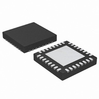
TDA8262HN/C1,118 NXP Semiconductors, TDA8262HN/C1,118 Datasheet - Page 8

TDA8262HN/C1,118
Manufacturer Part Number
TDA8262HN/C1,118
Description
IC SATELLITE TUNER 32-HVQFN
Manufacturer
NXP Semiconductors
Type
Satellite Tunerr
Datasheet
1.TDA8262HNC1118.pdf
(30 pages)
Specifications of TDA8262HN/C1,118
Package / Case
*
Applications
Demodulation
Mounting Type
Surface Mount
Bus Type
I2C
Maximum Agc
60 dB (Typ)
Maximum Frequency
2175 MHz
Minimum Frequency
950 MHz
Modulation Technique
QPSK
Mounting Style
SMD/SMT
Function
Satellite
Noise Figure
7.7 dB
Operating Supply Voltage
3.3 V
Supply Voltage (min)
3.15 V
Supply Voltage (max)
3.45 V
Minimum Operating Temperature
- 20 C
Maximum Operating Temperature
+ 85 C
Lead Free Status / RoHS Status
Lead free / RoHS Compliant
Lead Free Status / RoHS Status
Lead free / RoHS Compliant, Lead free / RoHS Compliant
Other names
935275321118
TDA8262HN/C1-T
TDA8262HN/C1-T
TDA8262HN/C1-T
TDA8262HN/C1-T
Philips Semiconductors
11. Programming
9397 750 13194
Product data sheet
10.1 Gain distribution
11.1 I
The output of the phase comparator drives the charge pump and loop amplifier section.
Pin CP is the output of the charge pump, and pin VT drives the tuning voltage to the
varicap diode of the voltage controlled oscillator. The loop filter has to be connected
between pins CP and VT.
For test and alignment purposes, it is possible to release the tuning voltage output and to
apply an external voltage on the VT pin, as well as to select the charge pump sink, source
or off.
Three independent area of power-down are available by programming I
The programming of the TDA8262HN is done through the I
selection is done through the R/W bit (address LSB). The TDA8262 fulfils the fast mode
I
9398 393 40011.
The I
3.3 V or 5.0 V, which allows direct connection to most of existing microcontrollers.
Data transfer format should be MSB first, and 8-bit word + acknowledge bit.
Pins used for the I
2
2
Fig 5. Gain distribution; typical values
•
•
•
C-bus specification, according to the Philips I
•
•
C-bus inputs
Loop-through part
RF and synthesizer part
Crystal oscillator and XTOUT part.
Pin SCL is the clock input
Pin SDA is the data input/output
2
C-bus lines SCL and SDA can be connected to an I
LNA /ATT
12 dB
RFATT
8 dB
2
C-bus:
Rev. 01 — 14 December 2004
AGC
AGC
dB
24
dB
37
10.2 dB
2
C-bus specification, see document
BBGAIN [ 3:0 ]
9 dB
Fully integrated satellite tuner
2
© Koninklijke Philips Electronics N.V. 2004. All rights reserved.
C-bus system tied to either
2
C-bus. The READ/WRITE
10.2 dB
TDA8262HN
10.2 dB
2
001aaa977
C-bus:
8 of 30


