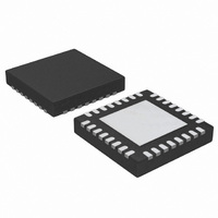
TDA8262HN/C1,118 NXP Semiconductors, TDA8262HN/C1,118 Datasheet - Page 23

TDA8262HN/C1,118
Manufacturer Part Number
TDA8262HN/C1,118
Description
IC SATELLITE TUNER 32-HVQFN
Manufacturer
NXP Semiconductors
Type
Satellite Tunerr
Datasheet
1.TDA8262HNC1118.pdf
(30 pages)
Specifications of TDA8262HN/C1,118
Package / Case
*
Applications
Demodulation
Mounting Type
Surface Mount
Bus Type
I2C
Maximum Agc
60 dB (Typ)
Maximum Frequency
2175 MHz
Minimum Frequency
950 MHz
Modulation Technique
QPSK
Mounting Style
SMD/SMT
Function
Satellite
Noise Figure
7.7 dB
Operating Supply Voltage
3.3 V
Supply Voltage (min)
3.15 V
Supply Voltage (max)
3.45 V
Minimum Operating Temperature
- 20 C
Maximum Operating Temperature
+ 85 C
Lead Free Status / RoHS Status
Lead free / RoHS Compliant
Lead Free Status / RoHS Status
Lead free / RoHS Compliant, Lead free / RoHS Compliant
Other names
935275321118
TDA8262HN/C1-T
TDA8262HN/C1-T
TDA8262HN/C1-T
TDA8262HN/C1-T
Philips Semiconductors
Table 39:
T
[1]
[2]
[3]
[4]
9397 750 13194
Product data sheet
Symbol
I
I
f
SDA output
V
AS input
I
I
PORTn
V
HI
LI
SCL
ASh
ASl
amb
Fig 6. Base band spectrum
O
O
The product is qualified with an output voltage of 550 mV (p-p) differential, however larger values can be used at baseband outputs that
might have impact on the product performance.
IIP
Wanted signal: RF1 is 2140 MHz, P
level is P1.
Unwanted signal: RF1 is 1040 MHz and P
on the output pins is P2.
IIP
Wanted signal: RF1 is LO + 5 MHz, P
Unwanted signal: RF1 is LO + 5 MHz and P
Phase noise in optimal conditions, see related application note.
= 25 C; V
2
3
= 20 + (P1
= 23 +
IM3 is the difference between the wanted signal and the unwanted signal (2f1
Characteristics
Parameter
HIGH-level leakage current
LOW-level leakage current
input clock frequency
output voltage during acknowledge
high level input current
low level input current
PORTn maximum output voltage
CC
IM3
---------- -
2
= 3.3 V; output level on differential I/Q output is 550 mV (p-p); unless otherwise specified.
P2) [dBm].
[dBm], see
…continued
Figure 6
RFIN
RFIN
= 20 dBm, and the AGC adjusted to get 550 mV (p-p) on the differential output. The output
RFIN
= 20 dBm, and the AGC adjusted to get 550 mV (p-p) on the differential output.
RFIN
3 MHz
= 20 dBm and RF2 is 1100 MHz and P
= 23 dBm and RF2 is LO + 7 MHz and Pin = 23 dBm
Rev. 01 — 14 December 2004
Conditions
V
V
I
V
V
I
sink
sink
5 MHz
IH
IL
AS
AS
f1
= 0 V; V
= 3.3 V; V
= 3 mA
= V
= 0 V
= 9 mA
CC
7 MHz
f2
CC
CC
= 3.3 V
= 0 V or 3.3 V
9 MHz
001aac085
IM3
f2) and (2f2
RFIN
= 20 dBm. The output level of (RF1 + RF2)
Fully integrated satellite tuner
© Koninklijke Philips Electronics N.V. 2004. All rights reserved.
Min
-
-
-
-
f1) on output pins
10
100
100
TDA8262HN
Typ
-
-
-
-
-
-
-
Max
-
400
0.4
+100
+100
0.4
10
Unit
kHz
V
V
A
A
A
A
23 of 30


