MM74HCT541MTCX Fairchild Semiconductor, MM74HCT541MTCX Datasheet
MM74HCT541MTCX
Specifications of MM74HCT541MTCX


Related parts for MM74HCT541MTCX


MM74HCT541MTCX Summary of contents
Page 1
... MTC20 MM74HCT541N N20A Devices also available in Tape and Reel. Specify by appending the suffix letter “X” to the ordering number. ©1984 Fairchild Semiconductor Corporation MM74HCT540, MM74HCT541 Rev. 1.3 General Description The MM74HCT540 and MM74HCT541 3-STATE buffers utilize advanced silicon-gate CMOS technology and are general purpose high speed inverting and non-inverting buffers ...
Page 2
... Connection Diagrams Pin Assignments for DIP, SOIC, SOP and TSSOP ©1984 Fairchild Semiconductor Corporation Rev. 1.3 Top View, MM74HCT540 Top View, MM74HCT541 2 www.fairchildsemi.com ...
Page 3
... Symbol V Supply Voltage Input or Output Voltage IN OUT T Operating Temperature Range Input Rise and Fall Times r f ©1984 Fairchild Semiconductor Corporation Rev. 1.3 (1) Parameter Parameter 3 Rating –0.5 to +7.0V –1 +1.5V CC –0 +0.5V CC ±20mA ±35mA ±70mA –65°C to +150°C ...
Page 4
... Minimum HIGH OH Level Output Voltage V Maximum LOW OL Level Voltage I Maximum Input IN Current I Maximum 3-STATE OZ Output Leakage Current I Maximum CC Quiescent Supply Current Note: 3. Measured per input. All other inputs at V ©1984 Fairchild Semiconductor Corporation Rev. 1 Conditions Typ 20µA V OUT 6.0mA, V 4.5V 4.2 ...
Page 5
... Maximum Input IN Capacitance C Maximum Output OUT Capacitance C Power Dissipation PD (4) Capacitance Note determines the no load dynamic power consumption current consumption ©1984 Fairchild Semiconductor Corporation Rev. 1.3 t 6ns, T 25°C, (unless otherwise specified Conditions C 45pF L C 45pF 5pF 6ns (unless otherwise specified). ...
Page 6
... Maximum Input IN Capacitance C Maximum Output OUT Capacitance C Power Dissipation PD (5) Capacitance Note determines the no load dynamic power consumption current consumption ©1984 Fairchild Semiconductor Corporation Rev. 1.3 t 6ns, T 25°C, (unless otherwise specified Conditions C 45pF L C 45pF 5pF 6ns (unless otherwise specified). r ...
Page 7
... Physical Dimensions Dimensions are in inches (millimeters) unless otherwise noted. Figure 1. 20-Lead Small Outline Integrated Circuit (SOIC), JEDEC MS-013, 0.300" Wide ©1984 Fairchild Semiconductor Corporation Rev. 1.3 Package Number M20B 7 www.fairchildsemi.com ...
Page 8
... Physical Dimensions (Continued) Dimensions are in millimeters unless otherwise noted. Figure 2. 20-Lead Small Outline Package (SOP), EIAJ TYPE II, 5.3mm Wide ©1984 Fairchild Semiconductor Corporation Rev. 1.3 Package Number M20D 8 www.fairchildsemi.com ...
Page 9
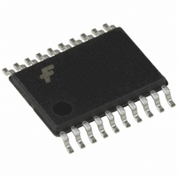
... Physical Dimensions (Continued) Dimensions are in millimeters unless otherwise noted. Figure 3. 20-Lead Thin Shrink Small Outline Package (TSSOP), JEDEC MO-153, 4.4mm Wide ©1984 Fairchild Semiconductor Corporation Rev. 1.3 Package Number MTC20 9 www.fairchildsemi.com ...
Page 10
... Physical Dimensions (Continued) Dimensions are in inches (millimeters) unless otherwise noted. Figure 4. 20-Lead Plastic Dual-In-Line Package (PDIP), JEDEC MS-001, 0.300" Wide ©1984 Fairchild Semiconductor Corporation Rev. 1.3 Package Number N20A 10 www.fairchildsemi.com ...
Page 11
... TRADEMARKS The following are registered and unregistered trademarks and service marks Fairchild Semiconductor owns or is authorized to use and is not intended exhaustive list of all such trademarks ® ACEx Build it Now™ CorePLUS™ CROSSVOLT™ CTL™ Current Transfer Logic™ ® ...