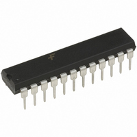
74F433SPC Fairchild Semiconductor, 74F433SPC Datasheet

74F433SPC
Specifications of 74F433SPC
Related parts for 74F433SPC
74F433SPC Summary of contents
Page 1
... The 74F433 has 3-STATE outputs that provide added ver- satility, and is fully compatible with all TTL families. Ordering Code: Order Number Package Number 74F433SPC N24C 24-Lead Plastic Dual-In-Line Package (PDIP), JEDEC MS-100, 0.300 Wide Logic Symbol © 1999 Fairchild Semiconductor Corporation ...
Page 2
Unit Loading/Fan Out Pin Names PL Parallel Load Input CPSI Serial Input Clock IES Serial Input Enable TTS Transfer to Stack Input MR Master Reset OES Serial Output Enable TOP Transfer Out Parallel TOS Transfer Out Serial CPSO Serial Output ...
Page 3
Functional Description As shown in the block diagram, the 74F433 consists of three sections Input Register with parallel and serial data inputs, as well as control inputs and outputs for input hand- shaking and expansion 4-bit-wide, ...
Page 4
FIGURE 2. Final Positions in an 74F433 Resulting from a 256-Bit Serial Train Fall-Through Stack—The outputs of flip-flops F the stack. A LOW level on the Transfer to Stack (TTS) input initiates a fall-through action; if the top location of ...
Page 5
FIGURE 3. Conceptual Output Section 5 www.fairchildsemi.com ...
Page 6
FIGURE 4. A Vertical Expansion Scheme Horizontal Expansion—The 74F433 can be horizontally expanded, without external logic, to store long words (in multiples of 4-bits). The interconnections necessary to form a 64-word by 12-bit FIFO are shown in Figure 5. Using ...
Page 7
FIFO resulting from a 2032-bit serial bit train. Interlocking Circuitry—Most conventional FIFO designs provide status signal analogous to IRF and ORE. However, when these devices are operated in arrays, variations in unit-to-unit operating ...
Page 8
FIGURE 7. Serial Data Entry for Array of Figure www.fairchildsemi.com FIGURE 6. A 127 x 16 FIFO Array 8 ...
Page 9
FIGURE 8. Serial Data Extraction for Array of Figure FIGURE 9. Final Position of a 2032-Bit Serial Input FIGURE 10. Conceptual Diagram, Interlocking Circuitry 9 www.fairchildsemi.com ...
Page 10
Absolute Maximum Ratings Storage Temperature Ambient Temperature under Bias Junction Temperature under Bias V Pin Potential to CC Ground Pin Input Voltage (Note 2) Input Current (Note 5.0 mA Voltage Applied to Output in HIGH State ...
Page 11
AC Electrical Characteristics Symbol Parameter t Propagation Delay, Negative-Going PHL CPSI to IRF Output t Propagation Delay, PLH Negative-Going TTS to IRF t Propagation Delay, Negative-Going PLH t CPSO to Q Output PHL S t Propagation Delay, Positive-Going PLH t ...
Page 12
AC Operating Requirements Symbol Parameter t (H) Setup Time, HIGH or LOW Negative CPSI (H) Hold Time, HIGH or LOW CPSI (L) Setup Time, ...
Page 13
Timing Waveforms Conditions: Stack not full, IES, PL LOW FIGURE 11. Serial Input, Unexpanded or Master Operation Conditions: Stack not full, IES HIGH when initiated, PL LOW FIGURE 12. Serial Input, Expanded Slave Operation Conditions: Data in stack, TOP HIGH, ...
Page 14
Timing Waveforms (Continued) Conditions: Data in stack, TOP HIGH, IES HIGH when initiated FIGURE 14. Serial Output, Slave Operation Conditions: IES LOW when initiated, OE, CPSO LOW; data available in stack FIGURE 15. Parallel Output, 4-Bit Word or Master in ...
Page 15
Timing Waveforms (Continued) Conditions: Stack not full, IES LOW when initialized NOTE A: TTS normally connected to IRF. NOTE B: If stack is full, IRF will stay LOW. FIGURE 17. Parallel Load Mode, 4-Bit Word (Unexpanded) or Master in Parallel ...
Page 16
Physical Dimensions inches (millimeters) unless otherwise noted 24-Lead Plastic Dual-In-Line Package (PDIP), JEDEC MS-100, 0.300 Wide Fairchild does not assume any responsibility for use of any circuitry described, no circuit patent licenses are implied and Fairchild reserves the right at ...


