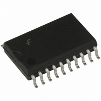
MM74HCT273WMX Fairchild Semiconductor, MM74HCT273WMX Datasheet - Page 4

MM74HCT273WMX
Manufacturer Part Number
MM74HCT273WMX
Description
IC FLIP FLOP OCTAL D 20-SOIC
Manufacturer
Fairchild Semiconductor
Series
74HCTr
Type
D-Type Busr
Datasheet
1.MM74HCT273WMX.pdf
(8 pages)
Specifications of MM74HCT273WMX
Function
Master Reset
Output Type
Non-Inverted
Number Of Elements
1
Number Of Bits Per Element
8
Frequency - Clock
68MHz
Delay Time - Propagation
22ns
Trigger Type
Positive Edge
Current - Output High, Low
4.8mA, 4.8mA
Voltage - Supply
4.5 V ~ 5.5 V
Operating Temperature
-40°C ~ 85°C
Mounting Type
Surface Mount
Package / Case
20-SOIC (7.5mm Width)
Logic Family
HCT
Technology
CMOS
Number Of Bits
8
Number Of Elements
1
Clock-edge Trigger Type
Positive-Edge
Polarity
Non-Inverting
Operating Supply Voltage (typ)
5V
Package Type
SOIC W
Propagation Delay Time
30ns
Low Level Output Current
4.8mA
High Level Output Current
-4.8mA
Frequency (max)
21MHz
Operating Supply Voltage (min)
4.5V
Operating Supply Voltage (max)
5.5V
Operating Temp Range
-40C to 85C
Operating Temperature Classification
Industrial
Mounting
Surface Mount
Pin Count
20
Lead Free Status / RoHS Status
Lead free / RoHS Compliant
Other names
MM74HCT273WMX
MM74HCT273WMXTR
MM74HCT273WMXTR
Available stocks
Company
Part Number
Manufacturer
Quantity
Price
Company:
Part Number:
MM74HCT273WMX
Manufacturer:
Fairchild Semiconductor
Quantity:
36 473
Part Number:
MM74HCT273WMX
Manufacturer:
FAIRCHILD/仙童
Quantity:
20 000
www.fairchildsemi.com
f
t
t
t
t
t
t
f
t
t
t
t
t
t
t
t
C
C
MAX
PHL
PHL
REM
S
H
W
MAX
PHL
PHL
REM
S
H
W
r
THL
Symbol
AC Electrical Characteristics
V
AC Electrical Characteristics
V
, t
Note 5: C
I
PD
IN
S
CC
CC
f
, t
, t
, t
, t
, t
Symbol
C
PLH
PLH
TLH
PLH
PLH
PD
5V, T
5.0V
V
PD
CC
Maximum Operating
Frequency
Maximum Propagation
Delay from Clock to Q
Maximum Propagation
Delay from Clear to Q
Minimum Removal
Time Clear to Clock
Minimum Set-Up Time
D to Clock
Minimum Hold Time
Clock to D
Minimum Pulse Width
Clock or Clear
Maximum Input Rise
and Fall Time, Clock
Maximum Output Rise
and Fall Time
Power Dissipation
Capacitance (Note 5)
Maximum Input
Capacitance
determines the no load dynamic power consumption, P
2
A
r
f
10%, C
I
CC
Maximum Operating Frequency
Maximum Propagation Delay from Clock to Q
Maximum Propagation Delay from Clear to Q
Minimum Removal Time, Clear to Clock
Minimum Set-Up Time D to Clock
Minimum Hold Time Clock to D
Minimum Pulse Width Clock or Clear
25
.
Parameter
q
C, C
L
L
50 pF, t
15 pF, t
Parameter
r
r
t
f
(Per Flip-Flop)
t
f
6 ns unless otherwise specified
6 ns
Conditions
D
C
PD
V
CC
4
2
Conditions
Typ
f
68
22
25
10
50
11
6
6
1
3
T
I
CC
A
V
25
CC
q
, and the no load dynamic current consumption,
C
500
27
37
35
20
16
15
10
5
5
T
A
Guaranteed Limits
40
Typ
68
18
21
10
500
21
46
44
25
25
19
10
6
q
6
5
1
3
C to 85
q
C T
Guaranteed
A
Limits
30
30
30
20
16
5
5
55
500
q
18
56
52
30
30
22
10
C to 125
7
5
q
Units
MHz
C Units
ns
ns
ns
ns
ns
ns
MHz
ns
ns
ns
ns
ns
ns
ns
ns
pF
pF


