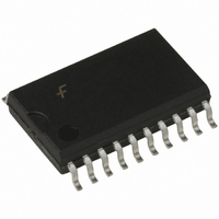
DM74ALS273WM Fairchild Semiconductor, DM74ALS273WM Datasheet - Page 3

DM74ALS273WM
Manufacturer Part Number
DM74ALS273WM
Description
IC FLIP FLOP OCT D POS 20SOIC
Manufacturer
Fairchild Semiconductor
Series
74ALSr
Type
D-Type Busr
Datasheet
1.DM74ALS273WM.pdf
(7 pages)
Specifications of DM74ALS273WM
Function
Master Reset
Output Type
Non-Inverted
Number Of Elements
1
Number Of Bits Per Element
8
Frequency - Clock
35MHz
Delay Time - Propagation
2ns
Trigger Type
Positive Edge
Current - Output High, Low
2.6mA, 24mA
Voltage - Supply
4.5 V ~ 5.5 V
Operating Temperature
0°C ~ 70°C
Mounting Type
Surface Mount
Package / Case
20-SOIC (7.5mm Width)
Logic Family
ALS
Technology
Bipolar
Number Of Bits
8
Number Of Elements
1
Clock-edge Trigger Type
Positive-Edge
Polarity
Non-Inverting
Operating Supply Voltage (typ)
5V
Package Type
SOIC W
Propagation Delay Time
18ns
Low Level Output Current
24mA
High Level Output Current
-2.6mA
Frequency (max)
35MHz
Operating Supply Voltage (min)
4.5V
Operating Supply Voltage (max)
5.5V
Operating Temp Range
0C to 70C
Operating Temperature Classification
Commercial
Mounting
Surface Mount
Pin Count
20
Lead Free Status / RoHS Status
Lead free / RoHS Compliant
Available stocks
Company
Part Number
Manufacturer
Quantity
Price
Company:
Part Number:
DM74ALS273WMX
Manufacturer:
NSC
Quantity:
13 250
V
V
V
I
I
f
t
t
t
t
T
f
t
t
t
V
V
V
I
I
I
I
I
OH
OL
CLK
W(CLK)
W
SU
H
MAX
PHL
PLH
PHL
I
IH
IL
O
CC
Absolute Maximum Ratings
Recommended Operating Conditions
Note 2: The ( ) arrow indicates the positive edge of the Clock is used for reference.
Electrical Characteristics
over recommended operating free air temperature range. All typical values are measured at V
Switching Characteristics
over recommended operating free air temperature range.
A
CC
IH
IL
IK
OH
OL
Symbol
Symbol
Supply Voltage
Input Voltage
Operating Free Air Temperature Range
Storage Temperature Range
Typical
Symbol
N Package
M Package
JA
Maximum Clock Frequency
Propagation Delay Time
HIGH-to-LOW Level Output
Propagation Delay Time
LOW-to-HIGH Level Output
Propagation Delay Time
HIGH-to-LOW Level Output
Input Clamp Voltage
HIGH Level
Output Voltage
LOW Level
Output Voltage
Input Current @ Maximum Input Voltage V
HIGH Level Input Current
LOW Level Input Current
Output Drive Current
Supply Current
Supply Voltage
HIGH Level Input Voltage
LOW Level Input Voltage
HIGH Level Output Current
LOW Level Output Current
Clock Frequency
Width of Clock Pulse
Width of Clear Pulse
Data Setup Time (Note 2)
Data Hold Time
Free Air Operating Temperature
Parameter
Parameter
Parameter
65 C to 150 C
V
R
C
CC
L
L
(Note 1)
0 C to 70 C
HIGH
LOW
LOW
Clear Inactive
V
V
V
V
V
V
V
V
Outputs OPEN
CC
CC
CC
CC
CC
CC
CC
CC
CC
500
50 pF
4.5V to 5.5V
60.0 C/W
79.0 C/W
4.5V, I
4.5V
4.5V to 5.5V
4.5V
5.5V, V
5.5V, V
5.5V, V
5.5V
5.5V
Conditions
7V
7V
I
IH
IH
IL
Conditions
3
18 mA
0.4V
7V
2.7V
Note 1: The “Absolute Maximum Ratings” are those values beyond which
the safety of the device cannot be guaranteed. The device should not be
operated at these limits. The parametric values defined in the Electrical
Characteristics tables are not guaranteed at the absolute maximum ratings.
The “Recommended Operating Conditions” table will define the conditions
for actual device operation.
Min
10
15
4.5
14
14
10
0
2
0
0
I
I
I
I
V
Outputs HIGH
Outputs LOW
OH
OH
OL
OL
O
From
Clear
Clock
Clock
2.25V
12 mA
24 mA
2.6 mA
400 A
CC
Nom
5
5V, T
V
Any Q
Any Q
Any Q
A
CC
Min
To
2.4
30
25 C.
2
0.25
0.35
Max
Typ
Min
3.3
5.5
0.8
19
11
35
24
35
70
2.6
4
2
3
www.fairchildsemi.com
Max
Max
0.4
0.5
0.1
20
112
20
29
18
1.5
0.2
12
15
Units
MHz
mA
mA
ns
ns
ns
ns
ns
V
V
V
C
Units
Units
MHz
mA
mA
mA
mA
mA
ns
ns
ns
V
V
V
V
V
A


