NC7WZ04L6X Fairchild Semiconductor, NC7WZ04L6X Datasheet - Page 3
NC7WZ04L6X
Manufacturer Part Number
NC7WZ04L6X
Description
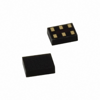
IC INVERTER UHS DUAL 6-MICROPAK
Manufacturer
Fairchild Semiconductor
Series
7WZr
Datasheet
1.NC7WZ04L6X.pdf
(9 pages)
Specifications of NC7WZ04L6X
Logic Type
Inverter
Number Of Inputs
1
Number Of Circuits
2
Current - Output High, Low
32mA, 32mA
Voltage - Supply
1.65 V ~ 5.5 V
Operating Temperature
-40°C ~ 85°C
Mounting Type
Surface Mount
Package / Case
6-MicroPak™
Logic Family
NC7WZ
High Level Output Current
- 32 mA
Low Level Output Current
32 mA
Supply Voltage (max)
5.5 V
Supply Voltage (min)
1.65 V
Maximum Operating Temperature
+ 85 C
Minimum Operating Temperature
- 40 C
Mounting Style
SMD/SMT
Operating Supply Voltage
1.65 V to 5.5 V
Lead Free Status / RoHS Status
Lead free / RoHS Compliant
Other names
NC7WZ04L6X
NC7WZ04L6XTR
NC7WZ04L6XTR
Available stocks
Company
Part Number
Manufacturer
Quantity
Price
Company:

Part Number:
NC7WZ04L6X
Manufacturer:
Fairchild Semiconductor
Quantity:
36 125
Company:
Part Number:
NC7WZ04L6X
Manufacturer:
CHILSIN
Quantity:
9 123
Part Number:
NC7WZ04L6X
Manufacturer:
FAIRCHILD/仙童
Quantity:
20 000


© 1999 Fairchild Semiconductor Corporation
NC7WZ04 • Rev. 1.0.2
Absolute Maximum Ratings
Stresses exceeding the absolute maximum ratings may damage the device. The device may not function or be
operable above the recommended operating conditions and stressing the parts to these levels is not recommended.
In addition, extended exposure to stresses above the recommended operating conditions may affect device
reliability. The absolute maximum ratings are stress ratings only.
Recommended Operating Conditions
The Recommended Operating Conditions table defines the conditions for actual device operation. Recommended
operating conditions are specified to ensure optimal performance to the datasheet specifications. Fairchild does not
recommend exceeding them or designing to Absolute Maximum Ratings.
Note:
4.
Symbol
I
Symbol
CC
V
V
t
Unused inputs must be held HIGH or LOW. They may not float.
V
V
T
ESD
θ
r
T
V
I
OUT
V
or I
I
, t
OUT
P
CC
T
T
JA
I
OUT
STG
IN
OK
A
CC
IK
IN
D
J
L
f
GND
Supply Voltage Operating
Supply Voltage Data Retention
Input Voltage
Output Voltage
Input Rise and Fall Times
Operating Temperature
Thermal Resistance
Supply Voltage
DC Input Voltage
DC Output Voltage
DC Input Diode Current
DC Output Diode Current
DC Output Source / Sink Current
DC V
Storage Temperature Range
Junction Temperature Under Bias
Junction Lead Temperature (Soldering, 10 Seconds)
Power Dissipation at +85°C
Human Body Model, JEDEC:JESD22-A114
Charge Device Model, JEDEC:JESD22-C101
CC
or Ground Current
Parameter
Parameter
V
V
SC70-6
MicroPak-6
MicroPak2-6
V
V
V
SC70-6
MicroPak-6
MicroPak2-6
IN
OUT
CC
CC
CC
< -0V
at 1.8V, 2.5V ±0.2V
at 3.3V ± 0.3V
at 5.0V ± 0.5V
< 0V
3
Conditions
Min.
-0.5
-0.5
-0.5
Min.
-65
1.65
-40
1.5
0
0
0
0
0
Max.
±100
+150
+150
+260
4000
2000
±50
180
130
120
7.0
7.0
7.0
-50
-50
Max.
5.50
+85
350
500
560
V
5.5
5.5
20
10
5
CC
www.fairchildsemi.com
Unit
mW
mA
mA
mA
mA
°C
°C
°C
°C/W
Unit
V
V
V
V
ns/V
°C
V
V
V
Related parts for NC7WZ04L6X
Image
Part Number
Description
Manufacturer
Datasheet
Request
R

Part Number:
Description:
Fairchild Semiconductor [IGBT MODULE]
Manufacturer:
Fairchild Semiconductor
Datasheet:

Part Number:
Description:
Discrete Semiconductor Modules
Manufacturer:
Fairchild Semiconductor
Part Number:
Description:
Discrete Semiconductor Modules
Manufacturer:
Fairchild Semiconductor
Part Number:
Description:
This N-Channel MOSFET is produced using Fairchild Semiconductor’s advanced Power Trench® process
Manufacturer:
Fairchild Semiconductor
Datasheet:
Part Number:
Description:
This N-Channel MOSFET is produced using Fairchild Semiconductor’s advanced Power Trench® process
Manufacturer:
Fairchild Semiconductor
Datasheet:
Part Number:
Description:
This N-Channel MOSFET is produced using Fairchild Semiconductor’s advanced PowerTrench® process
Manufacturer:
Fairchild Semiconductor
Datasheet:
Part Number:
Description:
This N-Channel MOSFET is produced using Fairchild Semiconductor’s advanced PowerTrench® process
Manufacturer:
Fairchild Semiconductor
Datasheet:
Part Number:
Description:
This N-Channel MOSFET is produced using Fairchild Semiconductor’s advanced Power Trench® process
Manufacturer:
Fairchild Semiconductor
Datasheet:
Part Number:
Description:
This N-Channel logic Level MOSFETs are produced using Fairchild Semiconductor‘s advanced Power Trench® process that has been special tailored to minimize the on-state resistance and yet maintain superior switching performance
Manufacturer:
Fairchild Semiconductor
Datasheet:
Part Number:
Description:
This N-Channel MOSFET is produced using Fairchild Semiconductor’s advanced Power Trench® process
Manufacturer:
Fairchild Semiconductor
Datasheet:
Part Number:
Description:
This N-Channel SyncFET™ is produced using Fairchild Semiconductor’s advanced PowerTrench® process
Manufacturer:
Fairchild Semiconductor
Datasheet:
Part Number:
Description:
This N-Channel SyncFET™ is produced using Fairchild Semiconductor’s advanced PowerTrench® process
Manufacturer:
Fairchild Semiconductor
Datasheet:
Part Number:
Description:
This N-Channel SyncFET™ is produced using Fairchild Semiconductor’s advanced PowerTrench® process
Manufacturer:
Fairchild Semiconductor
Datasheet:
Part Number:
Description:
This N-Channel logic Level MOSFETs are produced using Fairchild Semiconductor‘s advanced Power Trench® process that has been special tailored to minimize the on-state resistance and yet maintain superior switching performance
Manufacturer:
Fairchild Semiconductor
Datasheet:
Part Number:
Description:
This N-Channel MOSFET is produced using Fairchild Semiconductor’s advanced Power Trench® process that has been especially tailored to minimize the on-state resistance and yet maintain superior switching performance
Manufacturer:
Fairchild Semiconductor
Datasheet: