CD4023BCN Fairchild Semiconductor, CD4023BCN Datasheet
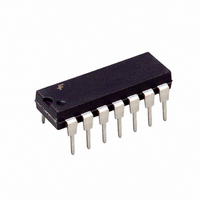
IC GATE NAND BUFF TRI 3INP 14DIP

CD4023BCN

Manufacturer Part Number
CD4023BCN
Description
IC GATE NAND BUFF TRI 3INP 14DIP
Manufacturer
Fairchild Semiconductor
Series
4000Br
Datasheet

Specifications of CD4023BCN

Logic Type
NAND Gate
Number Of Inputs
3
Number Of Circuits
3
Current - Output High, Low
8.8mA, 8.8mA
Voltage - Supply
3 V ~ 15 V
Operating Temperature
-55°C ~ 125°C
Mounting Type
Through Hole
Package / Case
14-DIP (0.300", 7.62mm)
Lead Free Status / RoHS Status
Lead free / RoHS Compliant
Other names
4023B
© 2004 Fairchild Semiconductor Corporation
CD4023BCM
(Note 1)
CD4023BCSJ
CD4023BCN
CD4023BC
Buffered Triple 3-Input NAND Gate
General Description
These triple gates are monolithic complementary MOS
(CMOS) integrated circuits constructed with N- and P-
channel enhancement mode transistors. They have equal
source and sink current capabilities and conform to stan-
dard B series output drive. The devices also have buffered
outputs which improve transfer characteristics by providing
very high gain. All inputs are protected against static dis-
charge with diodes to V
Ordering Code:
Note 1: Devices also available in Tape and Reel. Specify by appending the suffix letter “X” tot he ordering code.
Connection Diagram
Order Number
Package Number
DD
Top View
M14A
M14D
N14A
and V
SS
.
14-Lead Small Outline Integrated Circuit (SOIC), JEDEC MS-012, 0.150" Narrow
14-Lead Small Outline Package (SOP), EIAJ TYPE II, 5.3mm Wide
14-Lead Plastic Dual-In-Line Package (PDIP), JEDEC MS-001, 0.300" Wide
DS005956
Features
Block Diagram
1
*All Inputs Protected by Standard CMOS Input Protection Circuit.
/
3
Device Shown
Wide supply voltage range:
High noise immunity: 0.45 V
Low power TTL compatibility:
fan out of 2 driving 74L or 1 driving 74LS
5V–10V–15V parametric ratings
Symmetrical output characteristics
Maximum input leakage 1 A at 15V over full
temperature range
Package Description
October 1987
Revised January 2004
DD
3.0V to 15V
(typ)
www.fairchildsemi.com

Related parts for CD4023BCN

CD4023BCN Summary of contents

Page 1

... CD4023BCSJ M14D 14-Lead Small Outline Package (SOP), EIAJ TYPE II, 5.3mm Wide CD4023BCN N14A 14-Lead Plastic Dual-In-Line Package (PDIP), JEDEC MS-001, 0.300" Wide Note 1: Devices also available in Tape and Reel. Specify by appending the suffix letter “X” tot he ordering code. Connection Diagram Top View © ...

Page 2

Absolute Maximum Ratings (Note 3) DC Supply Voltage ( Input Voltage ( Storage Temp. Range ( Power Dissipation ( Dual-In-Line Small Outline Lead Temperature ( ...

Page 3

AC Electrical Characteristics pF 200k, unless otherwise specified Symbol Parameter t Propagation Delay, HIGH-to-LOW Level PHL t Propagation Delay, LOW-to-HIGH Level PLH t , Transition Time THL t TLH C Average ...

Page 4

Physical Dimensions inches (millimeters) unless otherwise noted 14-Lead Small Outline Integrated Circuit (SOIC), JEDEC MS-012, 0.150" Narrow www.fairchildsemi.com Package Number M14A 4 ...

Page 5

Physical Dimensions inches (millimeters) unless otherwise noted (Continued) 14-Lead Small Outline Package (SOP), EIAJ TYPE II, 5.3mm Wide Package Number M14D 5 www.fairchildsemi.com ...

Page 6

Physical Dimensions inches (millimeters) unless otherwise noted (Continued) 14-Lead Plastic Dual-In-Line Package (PDIP), JEDEC MS-001, 0.300" Wide Fairchild does not assume any responsibility for use of any circuitry described, no circuit patent licenses are implied and Fairchild reserves the right ...

Related keywords