MM74HC373SJX Fairchild Semiconductor, MM74HC373SJX Datasheet

IC LATCH OCTAL D 3-STATE 20-SOP

MM74HC373SJX

Manufacturer Part Number
MM74HC373SJX
Description
IC LATCH OCTAL D 3-STATE 20-SOP
Manufacturer
Fairchild Semiconductor
Series
74HCr
Type
D-Typer
Datasheet

Specifications of MM74HC373SJX

Logic Type
D-Type Transparent Latch
Circuit
8:8
Output Type
Tri-State
Voltage - Supply
2 V ~ 6 V
Independent Circuits
1
Delay Time - Propagation
19ns
Current - Output High, Low
7.8mA, 7.8mA
Operating Temperature
-40°C ~ 85°C
Mounting Type
Surface Mount
Package / Case
20-SOIC (7.5mm Width)
Logic Family
HC
Number Of Bits
8
Number Of Elements
1
Latch Mode
Transparent
Polarity
Non-Inverting
Technology
CMOS
Package Type
SOP W
Propagation Delay Time
280ns
Operating Supply Voltage (typ)
2.5/3.3/5V
High Level Output Current
-7.8mA
Low Level Output Current
7.8mA
Operating Supply Voltage (min)
2V
Operating Supply Voltage (max)
6V
Operating Temp Range
-40C to 85C
Operating Temperature Classification
Industrial
Mounting
Surface Mount
Pin Count
20
Lead Free Status / RoHS Status
Lead free / RoHS Compliant

Available stocks

Company
Part Number
Manufacturer
Quantity
Price
Part Number:
MM74HC373SJX
Manufacturer:
FAIRCHILD/仙童
Quantity:
20 000
© 2005 Fairchild Semiconductor Corporation
MM74HC373WM
MM74HC373SJ
MM74HC373MTC
MM74HC373N
MM74HC373
3-STATE Octal D-Type Latch
General Description
The MM74HC373 high speed octal D-type latches utilize
advanced silicon-gate CMOS technology. They possess
the high noise immunity and low power consumption of
standard CMOS integrated circuits, as well as the ability to
drive 15 LS-TTL loads. Due to the large output drive capa-
bility and the 3-STATE feature, these devices are ideally
suited for interfacing with bus lines in a bus organized sys-
tem.
When the LATCH ENABLE input is HIGH, the Q outputs
will follow the D inputs. When the LATCH ENABLE goes
LOW, data at the D inputs will be retained at the outputs
until LATCH ENABLE returns HIGH again. When a high
logic level is applied to the OUTPUT CONTROL input, all
outputs go to a high impedance state, regardless of what
signals are present at the other inputs and the state of the
storage elements.
The 74HC logic family is speed, function, and pin-out com-
patible with the standard 74LS logic family. All inputs are
protected from damage due to static discharge by internal
diode clamps to V
Ordering Code:
Devices also available in Tape and Reel. Specify by appending the suffix letter “X” to the ordering code.
Connection Diagram
Order Number
Pin Assignments for DIP, SOIC, SOP and TSSOP
CC
Package Number
and ground.
MTC20
Top View
M20D
M20B
N20A
20-Lead Small Outline Integrated Circuit (SOIC), JEDEC MS-013, 0.300" Wide
20-Lead Small Outline Package (SOP), EIAJ TYPE II, 5.3mm Wide
20-Lead Thin Shrink Small Outline Package (TSSOP), JEDEC MO-153, 4.4mm Wide
20-Lead Plastic Dual-In-Line Package (PDIP), JEDEC MS-001, 0.300" Wide
DS005335
Features
Truth Table
H
L
Q
Z
0
Typical propagation delay: 18 ns
Wide operating voltage range: 2 to 6 volts
Low input current: 1
Low quiescent current: 80
Output drive capability: 15 LS-TTL loads
LOW Level
High Impedance
HIGH Level
Level of output before steady-state input conditions were established.
Control
Output
Package Description
H
L
L
L
Enable
Latch
H
H
X
L
P
A maximum
P
A maximum (74 Series)
September 1983
Revised May 2005
Data
H
X
X
L
www.fairchildsemi.com
Output
373
Q
H
L
Z
0

Related parts for MM74HC373SJX

MM74HC373SJX Summary of contents

Page 1

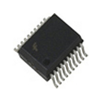
... Devices also available in Tape and Reel. Specify by appending the suffix letter “X” to the ordering code. Connection Diagram Pin Assignments for DIP, SOIC, SOP and TSSOP Top View © 2005 Fairchild Semiconductor Corporation Features Typical propagation delay Wide operating voltage range volts ...

Page 2

Absolute Maximum Ratings (Note 2) Supply Voltage ( Input Voltage ( Output Voltage (V ) OUT Clamp Diode Current ( Output Current, per pin (I ) ...

Page 3

AC Electrical Characteristics q 5V Symbol Parameter Maximum Propagation Delay, Data PHL PLH Maximum Propagation Delay ...

Page 4

AC Electrical Characteristics Symbol Parameter Conditions C Maximum Output OUT Capacitance Note 5: C determines the no load dynamic power consumption www.fairchildsemi.com (Continued ...

Page 5

Physical Dimensions inches (millimeters) unless otherwise noted 20-Lead Small Outline Integrated Circuit (SOIC), JEDEC MS-013, 0.300" Wide Package Number M20B 5 www.fairchildsemi.com ...

Page 6

Physical Dimensions inches (millimeters) unless otherwise noted (Continued) 20-Lead Small Outline Package (SOP), EIAJ TYPE II, 5.3mm Wide www.fairchildsemi.com Package Number M20D 6 ...

Page 7

Physical Dimensions inches (millimeters) unless otherwise noted (Continued) 20-Lead Thin Shrink Small Outline Package (TSSOP), JEDEC MO-153, 4.4mm Wide Package Number MTC20 7 www.fairchildsemi.com ...

Page 8

Physical Dimensions inches (millimeters) unless otherwise noted (Continued) 20-Lead Plastic Dual-In-Line Package (PDIP), JEDEC MS-001, 0.300" Wide Fairchild does not assume any responsibility for use of any circuitry described, no circuit patent licenses are implied and Fairchild reserves the right ...

Related keywords