CD4099BCN Fairchild Semiconductor, CD4099BCN Datasheet
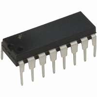
IC LATCH ADDRESSABLE 8BIT 16-DIP

CD4099BCN

Manufacturer Part Number
CD4099BCN
Description
IC LATCH ADDRESSABLE 8BIT 16-DIP
Manufacturer
Fairchild Semiconductor
Series
4000Br
Datasheet

Specifications of CD4099BCN

Logic Type
D-Type, Addressable
Circuit
1:8
Output Type
Standard
Voltage - Supply
3 V ~ 15 V
Independent Circuits
1
Delay Time - Propagation
50ns
Current - Output High, Low
8.8mA, 8.8mA
Operating Temperature
-55°C ~ 125°C
Mounting Type
Through Hole
Package / Case
16-DIP (0.300", 7.62mm)
Lead Free Status / RoHS Status
Lead free / RoHS Compliant
Other names
4099
4099B

Available stocks

Company
Part Number
Manufacturer
Quantity
Price
Part Number:
CD4099BCN
Manufacturer:
INTERSIL
Quantity:
926
© 2002 Fairchild Semiconductor Corporation
CD4099BCN
CD4099BC
8-Bit Addressable Latch
General Description
The CD4099BC is an 8-bit addressable latch with three
address inputs (A0–A2), an active low enable input (E),
active high clear input (CL), a data input (D), and eight out-
puts (Q0–Q7).
Data is entered into a particular bit in the latch when that bit
is addressed by the address inputs and the enable (E) is
LOW. Data entry is inhibited when enable (E) is HIGH.
When clear (CL) and enable (E) are HIGH, all outputs are
LOW. When clear (CL) is HIGH and enable (E) is LOW, the
channel demultiplexing occurs. The bit that is addressed
has an active output which follows the data input while all
unaddressed bits are held LOW. When operating in the
addressable latch mode (E
than one bit of the address could impose a transient wrong
address. Therefore, this should only be done while in the
memory mode (E
Ordering Code:
Connection Diagram
Truth Table
Order Number
Package Number
HIGH, CL
N16E
H
H H Reset to “0”
E CL
L
L
CL
H Follows Data
L Follows Data
L Holds Previous Data Holds Previous Data Memory
LOW).
LOW), changing more
16-Lead Plastic Dual-In-Line Package (PDIP), JEDEC MS-001, 0.300" Wide
Addressed
Latch
DS005984
Mode Selection
Top View
Holds Previous Data Addressable Latch
Reset to “0”
Reset to “0”
Unaddressed
Features
Latch
Wide supply voltage range:
High noise immunity: 0.45 V
Low power TTL: fan out of 2 driving 74L
Serial to parallel capability
Storage register capability
Random (addressable) data entry
Active high demultiplexing capability
Common active high clear
compatibility: or 1 driving 74LS
Package Description
Demultiplexer
Clear
Mode
October 1987
Revised April 2002
DD
3.0V to 15V
(typ.)
www.fairchildsemi.com

Related parts for CD4099BCN

CD4099BCN Summary of contents

Page 1

... Therefore, this should only be done while in the memory mode (E HIGH, CL LOW). Ordering Code: Order Number Package Number CD4099BCN N16E 16-Lead Plastic Dual-In-Line Package (PDIP), JEDEC MS-001, 0.300" Wide Connection Diagram Truth Table E CL Addressed Latch ...

Page 2

Logic Diagram www.fairchildsemi.com 2 ...

Page 3

Absolute Maximum Ratings (Note 2) DC Supply Voltage ( Input Voltage ( Storage Temperature Range ( Power Dissipation ( Dual-In-Line Small Outline Lead Temperature ( (Soldering, 10 ...

Page 4

AC Electrical Characteristics pF, R 200k, Input Symbol Parameter Propagation Delay PHL PLH Data to Output Propagation Delay PLH PHL Enable to Output t ...

Page 5

Switching Time Waveforms 5 www.fairchildsemi.com ...

Page 6

Physical Dimensions inches (millimeters) unless otherwise noted 16-Lead Plastic Dual-In-Line Package (PDIP), JEDEC MS-001, 0.300" Wide Fairchild does not assume any responsibility for use of any circuitry described, no circuit patent licenses are implied and Fairchild reserves the right at ...

Related keywords