MM74HC4538N Fairchild Semiconductor, MM74HC4538N Datasheet

IC MULTIVIBRATOR MONO DL 16-DIP

MM74HC4538N

Manufacturer Part Number
MM74HC4538N
Description
IC MULTIVIBRATOR MONO DL 16-DIP
Manufacturer
Fairchild Semiconductor
Series
74HCr
Datasheet

Specifications of MM74HC4538N

Logic Type
Monostable
Independent Circuits
2
Schmitt Trigger Input
Yes
Propagation Delay
26ns
Current - Output High, Low
5.2mA, 5.2mA
Voltage - Supply
2 V ~ 6 V
Operating Temperature
-40°C ~ 85°C
Mounting Type
Through Hole
Package / Case
16-DIP (0.300", 7.62mm)
Elements Per Chip
2
Logic Family
HC
Input Bias Current (max)
130 mA
Propagation Delay Time
275 ns, 55 ns, 47 ns
High Level Output Current
- 5.2 mA
Low Level Output Current
5.2 mA
Supply Voltage (max)
6 V
Supply Voltage (min)
2 V
Maximum Operating Temperature
+ 85 C
Minimum Operating Temperature
- 40 C
Mounting Style
Through Hole
Operating Supply Voltage
2.5 V, 3.3 V, 5 V
Lead Free Status / RoHS Status
Lead free / RoHS Compliant
Other names
74HC4538
© 2000 Fairchild Semiconductor Corporation
MM74HC4538M
MM74HC4538SJ
MM74HC4538N
MM74HC4538
Dual Retriggerable Monostable Multivibrator
General Description
The MM74HC4538 high speed monostable multivibrator
(one shots) is implemented in advanced silicon-gate
CMOS technology. They feature speeds comparable to low
power Schottky TTL circuitry while retaining the low power
and high noise immunity characteristic of CMOS circuits.
Each multivibrator features both a negative, A, and a posi-
tive, B, transition triggered input, either of which can be
used as an inhibit input. Also included is a clear input that
when taken low resets the one shot. The MM74HC4538 is
retriggerable. That is, it may be triggered repeatedly while
their outputs are generating a pulse and the pulse will be
extended.
Ordering Code:
Devices also available in Tape and Reel. Specify by appending the suffix letter “X” to the ordering code.
Connection Diagram
Order Number
Package Number
M16A
M16D
N16E
16-Lead Small Outline Integrated Circuit (SOIC), JEDEC MS-012, 0.150 Narrow
16-Lead Small Outline Package (SOP), EIAJ TYPE II, 5.3mm Wide
16-Lead Plastic Dual-In-Line Package (PDIP), JEDEC MS-001, 0.300 Wide
DS005217
Pulse width stability over a wide range of temperature and
supply is achieved using linear CMOS techniques. The out-
put pulse equation is simply: PW
in seconds, R is in ohms, and C is in farads. This device is
pin compatible with the CD4528, and the CD4538 one
shots. All inputs are protected from damage due to static
discharge by diodes to V
Features
Truth Table
H
L
X
Schmitt trigger on A and B inputs
Wide power supply range: 2–6V
Typical trigger propagation delay: 32 ns
Fanout of 10 LS-TTL loads
Low input current: 1 A max
LOW Level
Transition from LOW-to-HIGH
Transition from HIGH-to-LOW
Irrelevant
HIGH Level
One HIGH Level Pulse
One LOW Level Pulse
Clear
X
X
H
H
L
Package Description
Inputs
A
X
H
X
L
CC
and ground.
H
B
X
X
L
February 1984
Revised August 2000
0.7(R)(C) where PW is
www.fairchildsemi.com
Q
L
L
L
Outputs
Q
H
H
H

Related parts for MM74HC4538N

MM74HC4538N Summary of contents

Page 1

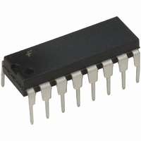
... Small Outline Integrated Circuit (SOIC), JEDEC MS-012, 0.150 Narrow MM74HC4538SJ M16D 16-Lead Small Outline Package (SOP), EIAJ TYPE II, 5.3mm Wide MM74HC4538N N16E 16-Lead Plastic Dual-In-Line Package (PDIP), JEDEC MS-001, 0.300 Wide Devices also available in Tape and Reel. Specify by appending the suffix letter “X” to the ordering code. ...

Page 2

Block Diagrams Note: Pin 1 and Pin 15 must be hard-wired to GND. Logic Diagram www.fairchildsemi.com 2 ...

Page 3

Timing Diagram Circuit Operation The MM74HC4538 operates as follows (refer to logic dia- gram). In the quiescent state, the external timing capacitor charged When a trigger occurs, the Q output X CC goes HIGH ...

Page 4

Circuit Operation (Continued) toggle, taking the Q output of the HC4538 to a LOW State (#19), and completing the time-out cycle. RESET OPERATION A low voltage applied to the Reset pin always forces the Q output of the HC4538 to ...

Page 5

Absolute Maximum Ratings (Note 2) Supply Voltage ( Input Voltage ( Output Voltage (V ) OUT Clamp Diode Current ( Output Current, per pin (I ) OUT DC ...

Page 6

DC Electrical Characteristics Note 5: The device must be set up with 3 steps before measuring I AC Electrical Characteristics 5V pF Symbol Parameter t ...

Page 7

AC Electrical Characteristics Symbol Parameter t Output Pulse Width Output Pulse Width Maximum Input IN Capacitance (Pins 2 & 14) C Maximum Input IN Capacitance (other inputs) C ...

Page 8

Physical Dimensions inches (millimeters) unless otherwise noted 16-Lead Small Outline Integrated Circuit (SOIC), JEDEC MS-012, 0.150 Narrow www.fairchildsemi.com Package Number M16A 8 ...

Page 9

Physical Dimensions inches (millimeters) unless otherwise noted (Continued) 16-Lead Small Outline Package (SOP), EIAJ TYPE II, 5.3mm Wide Package Number M16D 9 www.fairchildsemi.com ...

Page 10

Physical Dimensions inches (millimeters) unless otherwise noted (Continued) 16-Lead Plastic Dual-In-Line Package (PDIP), JEDEC MS-001, 0.300 Wide Fairchild does not assume any responsibility for use of any circuitry described, no circuit patent licenses are implied and Fairchild reserves the right ...

Related keywords