DM74LS221N Fairchild Semiconductor, DM74LS221N Datasheet

IC ONE-SHOT DL NON-RETRIG 16-DIP

DM74LS221N

Manufacturer Part Number
DM74LS221N
Description
IC ONE-SHOT DL NON-RETRIG 16-DIP
Manufacturer
Fairchild Semiconductor
Series
74LSr
Datasheet

Specifications of DM74LS221N

Logic Type
Monostable
Independent Circuits
2
Schmitt Trigger Input
Yes
Propagation Delay
65ns
Current - Output High, Low
400µA, 8mA
Voltage - Supply
4.75 V ~ 5.25 V
Operating Temperature
0°C ~ 70°C
Mounting Type
Through Hole
Package / Case
16-DIP (0.300", 7.62mm)
Lead Free Status / RoHS Status
Contains lead / RoHS non-compliant
Other names
74LS221
74LS221N

Available stocks

Company
Part Number
Manufacturer
Quantity
Price
Part Number:
DM74LS221N
Manufacturer:
01+
Quantity:
750
Part Number:
DM74LS221N
Manufacturer:
NS/国半
Quantity:
20 000
Part Number:
DM74LS221N*
Manufacturer:
national
Quantity:
500
© 2000 Fairchild Semiconductor Corporation
DM74LS221M
DM74LS221SJ
DM74LS221N
DM74LS221 Dual Non-Retriggerable One-Shot
with Clear and Complementary Outputs
General Description
The DM74LS221 is a dual monostable multivibrator with
Schmitt-trigger input. Each device has three inputs permit-
ting the choice of either leading-edge or trailing-edge trig-
gering. Pin (A) is an active-LOW trigger transition input and
pin (B) is an active-HIGH transition Schmitt-trigger input
that allows jitter free triggering for inputs with transition
rates as slow as 1 volt/second. This provides the input with
excellent noise immunity. Additionally an internal latching
circuit at the input stage also provides a high immunity to
V
pulse at a predetermined time independent of the timing
components. This (CLR) input also serves as a trigger
input when it is pulsed with a low level pulse transition
(
this device please read operating rules as well as the Fair-
child Semiconductor one-shot application notes carefully
and observe recommendations.
Ordering Code:
Devices also available in Tape and Reel. Specify by appending the suffix letter “X” to the ordering code.
Connection Diagram
Order Number
CC
). To obtain the best and trouble free operation from
noise. The clear (CLR) input can terminate the output
Package Number
M16D
M16A
N16E
16-Lead Small Outline Integrated Circuit (SOIC), JEDEC MS-012, 0.150 Narrow
16-Lead Small Outline Package (SOP), EIAJ TYPE II, 5.3mm Wide
16-Lead Plastic Dual-In-Line Package (PDIP), JEDEC MS-001, 0.300 Wide
DS006409
Features
Note 1: The pin-out is identical to DM74LS123 but, functionally it is not;
refer to Operating Rules #10 in this datasheet.
Function Table
H
L
X
Note 2: This mode of triggering requires first the B input be set from a
LOW-to-HIGH level while the CLEAR input is maintained at logic LOW
level. Then with the B input at logic HIGH level, the CLEAR input whose
positive transition from LOW-to-HIGH will trigger an output pulse.
A dual, highly stable one-shot
Compensated for V
Pin-out identical to DM74LS123 (Note 1)
Output pulse width range from 30 ns to 70 seconds
Hysteresis provided at (B) input for added noise
immunity
Direct reset terminates output pulse
Triggerable from CLEAR input
DTL, TTL compatible
Input clamp diodes
LOW Logic Level
Positive Going Transition
Negative Going Transition
Can Be Either LOW or HIGH
HIGH Logic Level
(Note 2)
CLEAR
A Positive Pulse
A Negative Pulse
Package Description
X
X
H
H
L
Inputs
A
X
H
X
L
L
CC
and temperature variations
August 1986
Revised April 2000
B
H
H
X
X
L
www.fairchildsemi.com
Q
L
L
L
Outputs
Q
H
H
H

Related parts for DM74LS221N

DM74LS221N Summary of contents

Page 1

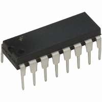
... Small Outline Integrated Circuit (SOIC), JEDEC MS-012, 0.150 Narrow DM74LS221SJ M16D 16-Lead Small Outline Package (SOP), EIAJ TYPE II, 5.3mm Wide DM74LS221N N16E 16-Lead Plastic Dual-In-Line Package (PDIP), JEDEC MS-001, 0.300 Wide Devices also available in Tape and Reel. Specify by appending the suffix letter “X” to the ordering code. ...

Page 2

Functional Description The basic output pulse width is determined by selection of an external resistor (R ) and capacitor (C X gered, the basic pulse width is independent of further input transitions and is a function of the timing components, ...

Page 3

... Operating Rules (Continued) FIGURE 1. FIGURE 3. FIGURE 5. Note: For further detailed device characteristics and output performance, please refer to the Fairchild Semiconductor one-shot application note AN-372. Note: “R ” should be as close to the one-shot as possible. remote FIGURE 2. FIGURE 4. FIGURE 6. 3 www.fairchildsemi.com ...

Page 4

Absolute Maximum Ratings Supply Voltage Input Voltage Operating Free Air Temperature Range Storage Temperature Range Recommended Operating Conditions Symbol Parameter V Supply Voltage CC V Positive-Going Input Threshold Voltage T at the A Input (V Min Negative-Going Input ...

Page 5

Electrical Characteristics over recommended operating free air temperature range (unless otherwise noted) Symbol Parameter V Input Clamp Voltage I V HIGH Level OH Output Voltage V LOW Level OL Output Voltage I Input Current @ Max Input Voltage I I ...

Page 6

Physical Dimensions inches (millimeters) unless otherwise noted 16-Lead Small Outline Integrated Circuit (SOIC), JEDEC MS-012, 0.150 Narrow www.fairchildsemi.com Package Number M16A 6 ...

Page 7

Physical Dimensions inches (millimeters) unless otherwise noted (Continued) 16-Lead Small Outline Package (SOP), EIAJ TYPE II, 5.3mm Wide Package Number M16D 7 www.fairchildsemi.com ...

Page 8

Physical Dimensions inches (millimeters) unless otherwise noted (Continued) 16-Lead Plastic Dual-In-Line Package (PDIP), JEDEC MS-001, 0.300 Wide Fairchild does not assume any responsibility for use of any circuitry described, no circuit patent licenses are implied and Fairchild reserves the right ...

Related keywords