DM74LS83AN Fairchild Semiconductor, DM74LS83AN Datasheet
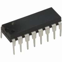
IC ADDER BIN W/CARRY 4BIT 16-DIP

DM74LS83AN

Manufacturer Part Number
DM74LS83AN
Description
IC ADDER BIN W/CARRY 4BIT 16-DIP
Manufacturer
Fairchild Semiconductor
Series
74LSr
Datasheet

Specifications of DM74LS83AN

Logic Type
Binary Full Adder
Supply Voltage
4.75 V ~ 5.25 V
Number Of Bits
4
Operating Temperature
0°C ~ 70°C
Mounting Type
Through Hole
Package / Case
16-DIP (0.300", 7.62mm)
Lead Free Status / RoHS Status
Contains lead / RoHS non-compliant
Other names
74LS83
74LS83AN
74LS83N
© 2000 Fairchild Semiconductor Corporation
DM74LS83AN
DM74LS83A
4-Bit Binary Adder with Fast Carry
General Description
These full adders perform the addition of two 4-bit binary
numbers. The sum ( ) outputs are provided for each bit
and the resultant carry (C4) is obtained from the fourth bit.
These adders feature full internal look ahead across all four
bits. This provides the system designer with partial look-
ahead performance at the economy and reduced package
count of a ripple-carry implementation.
The adder logic, including the carry, is implemented in its
true form meaning that the end-around carry can be
accomplished without the need for logic or level inversion.
Ordering Code:
Connection Diagram
Order Number
Package Number
N16E
16-Lead Plastic Dual-In-Line Package (PDIP), JEDEC MS-001, 0.300 Wide
DS006378
Features
Full-carry look-ahead across the four bits
Systems achieve partial look-ahead performance with
the economy of ripple carry
Typical add times
Typical power dissipation per 4-bit adder 95 mW
Two 8-bit words 25 ns
Two 16-bit words 45 ns
Package Description
August 1986
Revised March 2000
www.fairchildsemi.com

Related parts for DM74LS83AN

DM74LS83AN Summary of contents

Page 1

... Ordering Code: Order Number Package Number DM74LS83AN N16E 16-Lead Plastic Dual-In-Line Package (PDIP), JEDEC MS-001, 0.300 Wide Connection Diagram © 2000 Fairchild Semiconductor Corporation Features ...

Page 2

Truth Table H HIGH Level, L LOW Level Input conditions at A1, B1, A2, B2, and C0 are used to determine outputs 1 and 2 and the value of the internal carry C2. The values at C2, A3, B3, A4, ...

Page 3

Absolute Maximum Ratings Supply Voltage Input Voltage Operating Free Air Temperature Range Storage Temperature Range Recommended Operating Conditions Symbol Parameter V Supply Voltage CC V HIGH Level Input Voltage IH V LOW Level Input Voltage IL I HIGH Level Output ...

Page 4

Switching Characteristics and Symbol Parameter t Propagation Delay Time PLH LOW-to-HIGH Level Output t Propagation Delay Time PHL HIGH-to-LOW Level Output t Propagation Delay Time PLH LOW-to-HIGH Level Output t Propagation Delay ...

Page 5

Physical Dimensions inches (millimeters) unless otherwise noted 16-Lead Plastic Dual-In-Line Package (PDIP), JEDEC MS-001, 0.300 Wide Fairchild does not assume any responsibility for use of any circuitry described, no circuit patent licenses are implied and Fairchild reserves the right at ...

Related keywords