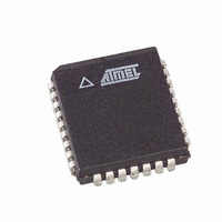
AT49LH002-33JC Atmel, AT49LH002-33JC Datasheet - Page 15

AT49LH002-33JC
Manufacturer Part Number
AT49LH002-33JC
Description
IC FLASH 2MBIT 33MHZ 32PLCC
Manufacturer
Atmel
Datasheet
1.AT49LH002-33JC.pdf
(36 pages)
Specifications of AT49LH002-33JC
Format - Memory
FLASH
Memory Type
FLASH
Memory Size
2M (256K x 8)
Speed
33MHz
Interface
Parallel
Voltage - Supply
3 V ~ 3.6 V
Operating Temperature
0°C ~ 85°C
Package / Case
32-PLCC
Lead Free Status / RoHS Status
Contains lead / RoHS non-compliant
Available stocks
Company
Part Number
Manufacturer
Quantity
Price
Response to
Invalid
FWH/LPC Fields
FWH Cycles
LPC Cycles
Bus Abort
3377B–FLASH–9/03
During FWH/LPC operations, the device will not explicitly indicate that it has received invalid
field sequences. The response to specific invalid fields or sequences is as follows:
•
•
•
Once valid START, IDSEL, and MSIZE fields are received, the device will always respond to
subsequent inputs as if they were valid. As long as the states of FWH/LAD[3:0] and
FWH4/LFRAME are known, the response of the device to signals received during the FWH
cycle should be predictable. The device will make no attempt to check the validity of incoming
Flash operation commands.
•
Once valid START and CYCTYPE + DIR fields are received, the device will always respond to
subsequent inputs as if they were valid. As long as the states of FWH/LAD[3:0] and
FWH4/LFRAME are known, the response of the device to signals received during the LPC
cycle should be predictable. The device will make no attempt to check the validity of incoming
Flash operation commands.
The Bus Abort operation can be used to immediately abort the current bus operation. A Bus
Abort occurs when FWH4/LFRAME is driven low for one or more clock cycles after the start of
a bus cycle. The memory will place the FWH/LAD[3:0] pins in a high-impedance state, and the
internal state machine will reset. During a write cycle, there is the possibility that an internal
Flash write or erase operation may be in progress (or has just been initiated). If the
FWH4/LFRAME pin is asserted during this time frame, the internal operation will not abort.
However, the internal state machine will not initiate a Flash write or erase operation until it has
received the last nibble from the host. This means that FWH4/LFRAME can be asserted as
late as clock cycle 12 (see Table 5 and Table 9) and no internal Flash operation will be
attempted.
When the FWH4/LFRAME pin has been driven low to abort a cycle, the host may issue a
START field of 1111b (stop/abort) to return the interface to the ready mode.
ID mismatch: If the IDSEL field does not match ID[3:0], then the device will ignore the
FWH cycle. The device will then enter standby mode when the FWH4/LFRAME pin is
brought high and no internal operation is in progress. The FWH/LAD[3:0] pins will also
be placed in a high-impedance state.
Address out of range: The FWH address sequences is seven fields long (28 bits), but
only the last six address fields (A23 - A0) will be decoded. Therefore, address bits
A27 - A24 will be ignored. In addition, because of the device density, address bits A23
and A21 - A18 will be ignored. Address bit A22 is used to determine whether reads or
writes to the device will be directed to the memory array (A22 = 1) or to the register
space (A22 = 0).
Invalid MSIZE field: If the device receives an invalid size field during a read or write
operation, the internal state machine will reset and no operation will be attempted. The
device will generate no response of any kind in this situation. Invalid size fields for a read
or write cycle are anything but 0000b. In addition, when accessing register space, invalid
field sizes are anything but 0000b.
Address out of range: The LPC address sequences is eight fields long (32 bits), but only
the last six address fields (A23 - A0) will be decoded. Therefore, address bits A31 - A24
will be ignored. In addition, because of the device density, address bits A22 - A18 will be
ignored. Address bit A23 is used to determine whether reads or writes to the device will be
directed to the memory array (A23 = 1) or to the register space (A23 = 0).
AT49LH002
15


