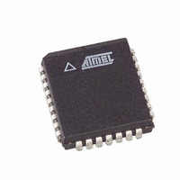
AT49LH002-33JC Atmel, AT49LH002-33JC Datasheet - Page 5

AT49LH002-33JC
Manufacturer Part Number
AT49LH002-33JC
Description
IC FLASH 2MBIT 33MHZ 32PLCC
Manufacturer
Atmel
Datasheet
1.AT49LH002-33JC.pdf
(36 pages)
Specifications of AT49LH002-33JC
Format - Memory
FLASH
Memory Type
FLASH
Memory Size
2M (256K x 8)
Speed
33MHz
Interface
Parallel
Voltage - Supply
3 V ~ 3.6 V
Operating Temperature
0°C ~ 85°C
Package / Case
32-PLCC
Lead Free Status / RoHS Status
Contains lead / RoHS non-compliant
Available stocks
Company
Part Number
Manufacturer
Quantity
Price
Table 1. Signal Descriptions (Continued)
3377B–FLASH–9/03
Symbol
I/O[7:0]
R/C
OE
WE
RDY/BSY
VCC
GND
NC
RES
Name and Function
DATA INPUTS/OUTPUTS: The I/O pins are used in the A/A Mux interface to input
data and commands during write cycles and to output data during memory array,
Status Register, and identifier code read cycles. Data is internally latched during a
write cycle.
The I/O pins will be in a high-impedance state when the outputs are disabled.
ROW/COLUMN ADDRESS SELECT: In the A/A Mux interface, the R/C pin is used
to latch the address values presented on the A[10:0] pins. The row addresses
(A10 - 0) are latched on the falling edge of R/C, and the column addresses
(A17 - A11) are latched on the rising edge of R/C.
OUTPUT ENABLE: The OE pin is used in the A/A Mux interface to control the
device’s output buffers during a read cycle.
The I/O[7:0] pins will be in high-impedance state when the OE pin is deasserted
(high).
WRITE ENABLE: The WE pin is used in the A/A Mux interface to control write
operations to the device.
READY/BUSY: The RDY/BSY pin provides the device’s ready/busy status when
using the A/A Mux interface. The RDY/BSY pin is a reflection of Status Register
bit 7, which is used to indicate whether a program or erase operation has been
completed.
Use of the RDY/BSY pin is optional, and the pin does not need to be connected.
DEVICE POWER SUPPLY: The VCC pin is used to supply the source voltage to
the device. Program and erase operations are inhibited when V
equal to V
Operations at invalid V
attempted.
GROUND: The ground reference for the power supply. GND should be connected
to the system ground.
NO CONNECT: NC pins have no internal connections and can be driven or left
floating. If the pins are driven, the voltage levels should comply with V
requirements.
RESERVED: RES pins are reserved for future device enhancements or
functionality. These pins may be left floating or may be driven. If the pins are driven,
the voltage levels should comply with V
These pins are used as the RDY/BSY and I/O[7:4] pins in the A/A Mux interface.
LKO
.
CC
voltages may produce spurious results and should not be
IH
and V
IL
requirements.
CC
is less than or
IH
and V
IL
FWH/LPC
X
X
X
X
Interface
AT49LH002
A/A Mux
X
X
X
X
X
X
X
X
X
Output
Output
Power
Power
Input/
Type
Input
Input
Input
–
–
5


