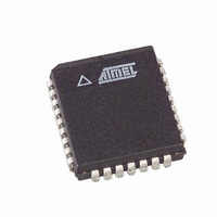
AT49LH002-33JC Atmel, AT49LH002-33JC Datasheet - Page 2

AT49LH002-33JC
Manufacturer Part Number
AT49LH002-33JC
Description
IC FLASH 2MBIT 33MHZ 32PLCC
Manufacturer
Atmel
Datasheet
1.AT49LH002-33JC.pdf
(36 pages)
Specifications of AT49LH002-33JC
Format - Memory
FLASH
Memory Type
FLASH
Memory Size
2M (256K x 8)
Speed
33MHz
Interface
Parallel
Voltage - Supply
3 V ~ 3.6 V
Operating Temperature
0°C ~ 85°C
Package / Case
32-PLCC
Lead Free Status / RoHS Status
Contains lead / RoHS non-compliant
Available stocks
Company
Part Number
Manufacturer
Quantity
Price
Block Diagram
2
AT49LH002
The sectoring of the AT49LH002’s memory array has been optimized to meet the needs of
today’s BIOS applications. By optimizing the size of the sectors, the BIOS code memory space
can be used more efficiently. Because certain BIOS code modules must reside in their own
sectors by themselves, the wasted and unused memory space that occurred with previous
generation BIOS Flash memory devices can be greatly reduced. This increased memory
space efficiency allows additional BIOS routines to be developed and added while still main-
taining the same overall device density.
The memory array of the AT49LH002 can be sectored in two ways simply by using two differ-
ent erase commands. Using one erase command allows the device to contain a total of seven
sectors comprised of a 16-Kbyte boot sector, two 8-Kbyte sectors, a 32-Kbyte sector, and
three 64-Kbyte sectors. The 16-Kbyte boot sector is located at the top (uppermost) of the
device’s memory address space and can be hardware write protected by using the TBL pin.
Alternatively, by using a different erase command, the memory array can be arranged into four
even erase sectors of 64-Kbyte each, allowing the top 64-Kbyte region to be used as the boot
sector. The TBL pin, when used with the second erase command, will hardware write protect
the entire top 64-Kbyte region against erasure.
The AT49LH002 supports two hardware interfaces: The FWH/LPC interface for In-System
operations and the A/A Mux interface for programming during manufacturing. The Interface
Configuration (IC) pin of the device provides the control between these two interfaces. An
internal Command User Interface (CUI) serves as the control center between the device inter-
faces and the internal operation of the nonvolatile memory. A valid command sequence
written to the CUI initiates device automation.
Specifically designed for use in 3-volt systems, the AT49LH002 supports read, program, and
erase operations with a supply voltage range of 3.0V to 3.6V. No separate voltage is required
for programming and erasing.
The AT49LH002 utilizes fixed program and erase times, independent of the number of pro-
gram and erase cycles that have occurred. Therefore, the system does not need to be
calibrated or correlated to the cumulative number of program and erase cycles.
FWH4/LFRAME
FWH/LAD[3:0]
RDY/BSY
GPI[4:0]
I/O[7:0]
A[10:0]
ID[3:0]
RST
CLK
R/C
WE
OE
IC
TBL
INTERFACE CONTROL
INTERFACE
INTERFACE
FWH/LPC
A/A MUX
WP
AND LOGIC
INIT
CONTROL LOGIC
X-DECODER
Y-DECODER
AND LATCHES
I/O BUFFERS
Y-GATING
MEMORY
FLASH
ARRAY
3377B–FLASH–9/03


