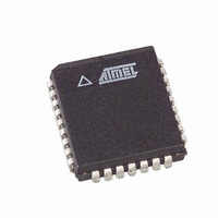
AT49LH002-33JC Atmel, AT49LH002-33JC Datasheet - Page 21

AT49LH002-33JC
Manufacturer Part Number
AT49LH002-33JC
Description
IC FLASH 2MBIT 33MHZ 32PLCC
Manufacturer
Atmel
Datasheet
1.AT49LH002-33JC.pdf
(36 pages)
Specifications of AT49LH002-33JC
Format - Memory
FLASH
Memory Type
FLASH
Memory Size
2M (256K x 8)
Speed
33MHz
Interface
Parallel
Voltage - Supply
3 V ~ 3.6 V
Operating Temperature
0°C ~ 85°C
Package / Case
32-PLCC
Lead Free Status / RoHS Status
Contains lead / RoHS non-compliant
Available stocks
Company
Part Number
Manufacturer
Quantity
Price
A/A Mux
Interface
3377B–FLASH–9/03
The A/A Mux interface is designed as a programming interface for OEMs to use during moth-
erboard manufacturing or component pre-programming. The term A/A Mux refers to the
multiplexed row and column addresses that this interface utilizes. The A/A Mux interface dra-
matically reduces the amount of overhead needed to access the device, allowing the device to
be tested and programmed quickly with automated test equipment (ATE) and PROM program-
mers in the OEM’s manufacturing flow. The number of signals required to use the interface
does not change with device density; therefore, the interface can accommodate larger density
devices while still allowing the device to fit into low lead-count packages.
Only basic read, erase, and program operations can be performed through the A/A Mux inter-
face; FWH/LPC features, such as the use of the Sector Locking Registers and the General-
purpose Input Register, are not available.
The A/A Mux interface mode is selected by driving the IC control pin high. The IC pin is inter-
nally pulled down in the device, so a modest amount of leakage current should be expected to
be drawn (see DC Specifications) when the pin is driven high.
Four control pins dictate the flow of data into and out of the device: R/C, OE, WE, and RST.
The R/C pin is the A/A Mux interface control pin used to latch row and column addresses. OE
is the data output control pin for the I/O[7:0] lines and, when active, drives the selected mem-
ory data onto the I/O bus (WE and RST must be at VIH). The WE pin controls the flow of data
into the device. Addresses previously captured by the R/C pin transitions and data are latched
into the device on the rising edge of WE. The RST pin is used to reset the device.
BUS OPERATION: All A/A Mux bus cycles can be conformed to operate on most automated
test equipment and PROM programmers.
Table 17. A/A Mux Interface Bus Operations
Notes:
OUTPUT DISABLE/ENABLE: With OE at a logic-high level (V
abled. Output pins I/O[7:0] are placed in the high-impedance state. With OE at a logic-low
level (V
state.
ROW/COLUMN ADDRESSES: R/C is the A/A Mux interface control pin used to latch row
(A10 - A0) and column address (A17-A11) values presented on the A[10:0] pins. R/C latches
row addresses on the falling edge and column addresses on the rising edge.
RDY/BSY: The open-drain Ready/Busy output pin provides a hardware method of detecting
the end of a program or erase operation. RDY/BSY is actively pulled low during the internal
program and erase cycles and is released at the completion of the cycle.
Mode
Read
Output Disable
Write
Product ID Read
(1)(2)
(1)(2)
IL
1. X can be V
2. V
3. Refer to Table 20 for Product ID addresses and data.
), the device outputs are enabled. Output pins I/O[7:0] are placed in an output-drive
V
IH
IL
min = 0.5V, V
(1)(2)
and V
(1)(2)(3)
IL
IL
refer to the DC characteristics associated with the Flash memory output buffers:
or V
IL
IH
max = 0.8V, V
for control and address input pins.
RST
V
V
V
V
IH
IH
IH
IH
IH
min = 2.0V, V
OE
V
V
V
V
IH
IH
IL
IL
IH
max = V
WE
V
V
V
V
IH
IH
IH
IL
IH
CC
), the device outputs are dis-
+ 0.5V.
Address
Note 3
AT49LH002
X
X
X
I/O[7:0]
High-Z
Note 3
D
D
OUT
IN
21


