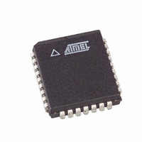
AT49LH002-33JC Atmel, AT49LH002-33JC Datasheet - Page 3

AT49LH002-33JC
Manufacturer Part Number
AT49LH002-33JC
Description
IC FLASH 2MBIT 33MHZ 32PLCC
Manufacturer
Atmel
Datasheet
1.AT49LH002-33JC.pdf
(36 pages)
Specifications of AT49LH002-33JC
Format - Memory
FLASH
Memory Type
FLASH
Memory Size
2M (256K x 8)
Speed
33MHz
Interface
Parallel
Voltage - Supply
3 V ~ 3.6 V
Operating Temperature
0°C ~ 85°C
Package / Case
32-PLCC
Lead Free Status / RoHS Status
Contains lead / RoHS non-compliant
Available stocks
Company
Part Number
Manufacturer
Quantity
Price
Device Memory Map
Pin Description
Table 1 provides a description of each of the device pins. Most of the pins have dual functionality in that they are used for
both the FWH/LPC interface as well as the A/A Mux interface.
Table 1. Signal Descriptions
3377B–FLASH–9/03
Symbol
IC
CLK
FWH4/
LFRAME
FWH/
LAD[3:0]
RST
Sector
6
5
4
3
2
1
0
Name and Function
INTERFACE COMMUNICATION: The IC pin determines which interface is
operational. If the IC pin is held high, then the A/A Mux interface is enabled, and if
the IC pin is held low, then the FWH/LPC interface is enabled. The IC pin must be
set at power-up or before returning from a reset condition and cannot be changed
during device operation.
The IC pin is internally pulled-down with a resistor valued between 20 kΩ and
100 kΩ, so connection of this pin is not necessary if the FWH/LPC interface will
always be used in the system. If the IC pin is driven high to enable the A/A Mux
interface, then the pin will exhibit some leakage current.
FWH/LPC CLOCK: This pin is used to provide a clock to the device. This pin is
usually connected to the 33 MHz PCI clock and adheres to the PCI specification.
This pin is used as the R/C pin in the A/A Mux interface.
FWH INPUT/LPC FRAME: This pin is used to indicate the start of a FWH or LPC
data transfer operation. The pin is also used to abort a FWH or LPC cycle in
progress.
This pin is used as the WE pin in the A/A Mux interface.
FWH/LPC ADDRESS AND DATA: These pins are used for FWH/LPC bus
information such as addresses, data, and command inputs/outputs.
These pins are used as the I/O[3:0] pins in the A/A Mux interface.
INTERFACE RESET: The RST pin is used for both FWH/LPC and A/A Mux
interfaces. When the RST pin is driven low, write operations are inhibited, internal
automation is reset, and the FWH/LAD[3:0] pins (when using the FWH/LPC
interface) are put into a high-impedance state. When the device exits the reset
state, it will default to the read array mode.
Main Sector
Main Sector
Main Sector
Sub-sector
Sub-sector
Sub-sector
Sub-sector
Type
Size (Bytes)
16K
32K
64K
64K
64K
8K
8K
03C000H - 03FFFFH
03A000H - 03BFFFH
038000H - 039FFFH
030000H - 037FFFH
020000H - 02FFFFH
010000H - 01FFFFH
000000H - 00FFFFH
FWH/LPC
Address Range
X
X
X
X
X
Interface
AT49LH002
A/A Mux
X
X
Output
Input/
Type
Input
Input
Input
Input
3


