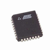
AT49LH002-33JC Atmel, AT49LH002-33JC Datasheet - Page 16

AT49LH002-33JC
Manufacturer Part Number
AT49LH002-33JC
Description
IC FLASH 2MBIT 33MHZ 32PLCC
Manufacturer
Atmel
Datasheet
1.AT49LH002-33JC.pdf
(36 pages)
Specifications of AT49LH002-33JC
Format - Memory
FLASH
Memory Type
FLASH
Memory Size
2M (256K x 8)
Speed
33MHz
Interface
Parallel
Voltage - Supply
3 V ~ 3.6 V
Operating Temperature
0°C ~ 85°C
Package / Case
32-PLCC
Lead Free Status / RoHS Status
Contains lead / RoHS non-compliant
Available stocks
Company
Part Number
Manufacturer
Quantity
Price
Device Reset
Sector
Protection
Hardware Write
Protection
16
AT49LH002
Asserting RST or INIT initiates a device reset. In read mode, RST or INIT low deselects the
memory, places the output drivers in a high-impedance state, and turns off all internal circuits.
RST or INIT must be held low for the minimum specified t
operations). The device resets to read array mode upon return from reset, and all Sector Lock-
ing Registers are reset to their default (write-locked) state. Since all Sector Locking Registers
are reset, all sectors in the memory array are set to the write-locked status regardless of their
locked state prior to reset.
A reset recovery time (t
face) is required from RST or INIT switching back high until writes to the CUI are recognized.
A reset latency will occur if a reset procedure is performed during a programming or erase
operation.
During sector erase or program, driving RST or INIT low will abort the operation underway in
addition to causing a reset latency. Memory contents being altered are no longer valid since
the data may be partially erased or programmed.
It is important to assert RST or INIT during system reset. When the system comes out of reset,
it will expect to read from the memory array of the device. If a system reset occurs with no
FWH/LPC device reset (this will be hardware dependent), it is possible that proper CPU initial-
ization will not occur (the FWH/LPC memory may be providing status information instead of
memory array data).
Sectors in the memory array can be protected from program and erase operations using a
hardware controlled method and/or a software (register-based) controlled method.
Two pins are available to provide hardware write protection capabilities. The Top Boot Sector
Lock (TBL) pin, when held low, prevents program and sector erase operations to the top sec-
tor of the device (sector 6) where critical code can be stored. In addition, the TBL pin has the
flexibility to provide erase protection to the top 64-Kbyte region (sectors 6, 5, 4, and 3) of the
device when the Uniform Sector Erase command is used. This allows the TBL pin to protect a
larger region for systems that require a 64-Kbyte top boot sector rather than a 16-Kbyte top
boot sector.
When the TBL pin is high, hardware write protection for program and erase operations to the
top sector is disabled. Provided that the Write-Lock bits in the Sector Locking Registers are
not set (detailed later), sector erase commands can then be issued to the device to erase
either the top 16-Kbyte sector (sector 6) or the entire top 64-Kbyte region (sectors 6, 5, 4,
and 3). Program operations can also be performed to the top 16-Kbyte sector.
The Write Protect (WP) pin, which operates independently from the TBL pin, serves the same
basic function as the TBL pin for the remaining sectors except the top boot sector. When the
WP pin is held low, program and standard Sector Erase command operations to sectors 5
through 0 will not be allowed. If using the Uniform Sector Erase command, then erase opera-
tions to sectors 2, 1, and 0 cannot be performed, and erase protection for sectors 6 through 3
will be controlled by the TBL pin.
PHFV
using the FWH/LPC interface and t
PLPH
time (FWH/LPC and A/A Mux
PHAV
using the A/A Mux inter-
3377B–FLASH–9/03


