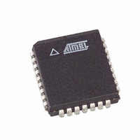
AT49LH002-33JC Atmel, AT49LH002-33JC Datasheet - Page 6

AT49LH002-33JC
Manufacturer Part Number
AT49LH002-33JC
Description
IC FLASH 2MBIT 33MHZ 32PLCC
Manufacturer
Atmel
Datasheet
1.AT49LH002-33JC.pdf
(36 pages)
Specifications of AT49LH002-33JC
Format - Memory
FLASH
Memory Type
FLASH
Memory Size
2M (256K x 8)
Speed
33MHz
Interface
Parallel
Voltage - Supply
3 V ~ 3.6 V
Operating Temperature
0°C ~ 85°C
Package / Case
32-PLCC
Lead Free Status / RoHS Status
Contains lead / RoHS non-compliant
Available stocks
Company
Part Number
Manufacturer
Quantity
Price
Interface
Selection
FWH/LPC
Interface
6
AT49LH002
The AT49LH002 can operate in two distinct interface modes: The FWH/LPC interface and the
A/A Mux interface. Selection of the interface is determined by the state of the IC pin. When the
IC pin is held low, the device will operate using the FWH/LPC interface. Alternatively, when
the IC pin is held high, the device will operate using the A/A Mux interface.
The FWH/LPC interface is designed as an In-System interface used in communicating with
either the I/O Controller Hub (ICH) in Intel chipsets or typically the PCI south bridge in non-
Intel chipsets.
The FWH/LPC interface uses a 5-signal communication interface consisting of a 4-bit data
bus, the FWH/LAD[3:0] pins, and one control line, the FWH4/LFRAME pin. The operation and
timing of the interface is based on the 33 MHz PCI clock, and the buffers for the FWH/LPC
interface are PCI compliant. To ensure the effective delivery of security and manageability fea-
tures, the FWH/LPC interface is the only way to get access to the full feature set of the device.
Commands, addresses, and data are transferred via the FWH/LPC interface using a series of
fields. The field sequences and contents are strictly defined for FWH and LPC memory cycles.
These field sequences are detailed in the FWH Interface Operation and LPC Interface Opera-
tion sections.
Since the AT49LH002 can be used as either a FWH Flash or an LPC Flash, the device is
capable of automatically detecting which type of memory cycle is being performed. For a
FWH/LPC cycle, the host will drive the FWH4/LFRAME pin low for one or more clock cycles to
initiate the operation. After driving the FWH4/LFRAME pin low, the host will send a START
value to indicate the type of FWH/LPC cycle that is to be performed. The value of the START
field determines whether the device will operate using a FWH cycle or an LPC cycle. Table 2
details the three valid START fields that the device will recognize.
Table 2. FWH/LPC Start Fields
If a valid START value is not detected, then the device will enter standby mode when the
FWH4/LFRAME pin is high and no internal operation is in progress. The FWH/LAD[3:0] pins
will also be placed in a high-impedance state.
FWH4/LFRAME PIN: FWH4/LFRAME is used by the master to indicate the start of cycles and
the termination of cycles due to an abort or time-out condition. This signal is to be used by
peripherals to know when to monitor the bus for a cycle.
The FWH4/LFRAME signal is used as a general notification that the FWH/LAD[3:0] lines con-
tain information relative to the start or stop of a cycle, and that peripherals must monitor the
bus to determine whether the cycle is intended for them. The benefit to peripherals of
FWH4/LFRAME is that it allows them to enter lower power states internally when a cycle is not
intended for them.
When peripherals sample FWH4/LFRAME is active, they are to immediately stop driving the
FWH/LAD[3:0] signal lines on the next clock and monitor the bus for new cycle information.
START Value
0000b
1101b
1110b
Cycle Type
LPC Cycle – The type (memory, I/O, DMA) and direction of the cycle (read or
write) is determined by the second field (CYCTYPE + DIR) of the LPC cycle. Only
memory cycles are supported by the device.
FWH Memory Read Cycle
FWH Memory Write Cycle
3377B–FLASH–9/03


