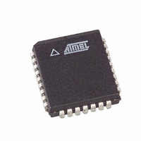
AT49LW080-33JC SL383 Atmel, AT49LW080-33JC SL383 Datasheet - Page 12

AT49LW080-33JC SL383
Manufacturer Part Number
AT49LW080-33JC SL383
Description
IC FLASH 8MBIT 33MHZ 32PLCC
Manufacturer
Atmel
Datasheet
1.AT49LW080-33JC.pdf
(34 pages)
Specifications of AT49LW080-33JC SL383
Format - Memory
FLASH
Memory Type
FLASH
Memory Size
8M (1M x 8)
Speed
33MHz
Interface
Parallel
Voltage - Supply
3 V ~ 3.6 V
Operating Temperature
0°C ~ 85°C
Package / Case
32-PLCC
Lead Free Status / RoHS Status
Contains lead / RoHS non-compliant
6.3
6.4
6.5
6.6
12
Output Disable
Response to Invalid Fields
Bus Abort
Hardware Write-protect Pins TBL and WP
AT49LW080
When the FWH is not selected through a FWH read or write cycle, the FWH interface outputs
(FWH[3:0]) are disabled and will be placed in a high-impedance state.
During FWH operations, the FWH will not explicitly indicate that it has received invalid field
sequences. The response to specific invalid fields or sequences is as follows:
The Bus Abort operation can be used to immediately abort the current bus operation. A Bus
Abort occurs when FWH4 is driven Low, V
the Input/Output Communication pins, FWH3 - FWH0 and the FWH state machine will reset.
During a write cycle, there is the possibility that an internal Flash write or erase operation is in
progress (or has just been initiated). If the FWH4 is asserted during this time frame, the internal
operation will not abort. The software must send an explicit Flash command to terminate or sus-
pend the operation. The internal FWH state machine will not initiate a Flash write or erase
operation until it has received the last nibble from the chipset. This means that FWH4 can be
asserted as late as cycle 12
Two pins are available with the FWH to provide hardware write-protect capabilities.
The Top Sector Lock (TBL) pin is a signal, when held low (active), prevents program or sector
erase operations in the top sector of the device (15) where critical code can be stored. When
TBL is high, hardware write protection of the top sector is disabled. The write-protect (WP) pin
serves the same function for all the remaining sectors except the top sector. WP operates inde-
pendently from TBL and does not affect the lock status of the top sector.
The TBL and WP pins must be set to the desired protection state prior to starting a program or
erase operation since they are sampled at the beginning of the operation. Changing the state of
TBL or WP during a program or erase operation may cause unpredictable results.
If the state of TBL or WP changes during a program suspend or erase suspend state, the
changes to the device’s locking status do not take place immediately. The suspended operation
• Address out of range: The FWH address sequences is seven fields long (28 bits), but only
• Invalid MSIZE field: If the FWH receives an invalid size field during a read or write operation,
the last five address fields (20 bits) will be decoded by an 8-Mbit FWH. The FWH will respond
to these lower addresses, regardless of the value of the more-significant address bits.
Address A22 has the special function of directing reads and writes to the Flash core (A22 =
1) or to the register space (A22 = 0).
the internal state machine will reset and no operation will be attempted. The FWH will
generate no response of any kind in this situation. Invalid-size fields for a read cycle are
anything but 0000. Invalid-size fields for a write cycle are anything but 0000. When accessing
register space, invalid field sizes are anything but 0000.
Once valid START, IDSEL, and MSIZE fields are received, the FWH always will respond to
subsequent inputs as if they were valid. As long as the states of FWH [3:0] and FWH4 are
known, the response of the FWH to signals received during the FWH cycle should be predict-
able. The FWH will make no attempt to check the validity of incoming Flash operation
commands.
(Table
6-3) and no internal Flash operation will be attempted.
IL
, during the bus operation; the memory will tri-state
1966G–FLASH–3/05


