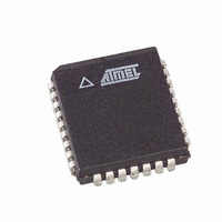
AT49LW080-33JC SL383 Atmel, AT49LW080-33JC SL383 Datasheet - Page 6

AT49LW080-33JC SL383
Manufacturer Part Number
AT49LW080-33JC SL383
Description
IC FLASH 8MBIT 33MHZ 32PLCC
Manufacturer
Atmel
Datasheet
1.AT49LW080-33JC.pdf
(34 pages)
Specifications of AT49LW080-33JC SL383
Format - Memory
FLASH
Memory Type
FLASH
Memory Size
8M (1M x 8)
Speed
33MHz
Interface
Parallel
Voltage - Supply
3 V ~ 3.6 V
Operating Temperature
0°C ~ 85°C
Package / Case
32-PLCC
Lead Free Status / RoHS Status
Contains lead / RoHS non-compliant
5. Firmware Hub Interface (FWH)
5.1
5.2
5.3
6
FWH[3:0]
FWH4
Reset
AT49LW080
Table 5-1
Table 5-1.
The FWH[3:0] signal lines communicate address, control, and data information over the LPC
bus between a master and a peripheral. The information communicated are: start, stop (abort a
cycle), transfer type (memory, I/O, DMA), transfer direction (read/write), address, data, wait
states, DMA channel, and bus master grant.
FWH4 is used by the master to indicate the start of cycles and the termination of cycles due to
an abort or time-out condition. This signal is to be used by peripherals to know when to monitor
the bus for a cycle.
The FWH4 signal is used as a general notification that the FWH[3:0] lines contain information
relative to the start or stop of a cycle, and that peripherals must monitor the bus to determine
whether the cycle is intended for them. The benefit to peripherals of FWH4 is, it allows them to
enter lower power states internally.
When peripherals sample FWH4 active, they are to immediately stop driving the FWH[3:0] signal
lines on the next clock and monitor the bus for new cycle information.
RST or INIT at VIL initiates a device reset. In read mode, RST or INIT low deselects the mem-
ory, places output drivers in a high-impedance state, and turns off all internal circuits. RST or
INIT must be held low for time t
array mode upon return from reset, and all sectors are set to default (locked) status regardless
of their locked state prior to reset.
Driving RST or INIT low resets the device, which resets the sector lock registers to their default
(write-locked) condition. A reset time (t
high until outputs are valid. Likewise, the device has a wake time (t
INIT high until writes to the CUI are recognized. A reset latency will occur if a reset procedure is
performed during a programming or erase operation.
Signal
FWH[3:0]
FWH4
RST
CLK
lists the seven required signals used for the FWH interface.
FWH Required Signal List
Peripheral
I/O
I
I
I
Direction
Master
PLPH
I/O
O
I
I
(A/A Mux and FWH operation). The FWH resets to read
PHQV
Description
Multiplexed command, address and data
Indicates start of a new cycle, termination of broken cycle.
Reset: Same as PCI Reset on the master. The master does
not need this signal if it already has PCIRST on its
interface.
Clock: Same 33 MHz clock as PCI clock on the master.
Same clock phase with typical PCI skew. The master does
not need this signal if it already has PCICLK on its
interface.
A/A Mux) is required from RST or INIT switching
PHRH
A/A Mux) from RST or
1966G–FLASH–3/05


