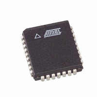
AT49LW080-33JC SL383 Atmel, AT49LW080-33JC SL383 Datasheet - Page 8

AT49LW080-33JC SL383
Manufacturer Part Number
AT49LW080-33JC SL383
Description
IC FLASH 8MBIT 33MHZ 32PLCC
Manufacturer
Atmel
Datasheet
1.AT49LW080-33JC.pdf
(34 pages)
Specifications of AT49LW080-33JC SL383
Format - Memory
FLASH
Memory Type
FLASH
Memory Size
8M (1M x 8)
Speed
33MHz
Interface
Parallel
Voltage - Supply
3 V ~ 3.6 V
Operating Temperature
0°C ~ 85°C
Package / Case
32-PLCC
Lead Free Status / RoHS Status
Contains lead / RoHS non-compliant
5.4.3
5.4.4
5.4.5
6. Device Operation
6.1
6.1.1
8
Read
AT49LW080
IDSEL (Device Select)
MADDR (Memory Address)
MSIZE (Memory Size)
Read Cycle, Single Byte
This one-clock field is used to indicate which FWH component is being selected. The four bits
transmitted over FWH[3:0] during this clock are compared with values strapped onto pins
[ID3:ID0] on the FWH component. If there is a match, the FWH component will continue to
decode the cycle to determine which bytes are requested on a read or which bytes to update on
a write. If there isn’t a match, the FWH component may discard the rest of the cycle and go into
a standby power state.
This is a seven-clock field, which gives a 28-bit memory address. This allows for up to 256 MB
per memory device, for a total of a 4 GB addressable space. The address is transferred with the
most significant nibble first.
“0000b” will be sent in this field. A value of “0000b” corresponds to a single byte transfer.
Read operations consist of preamble, TAR, SYNC and data fields as shown in
described in
mode include the following functions: reading memory from the array, reading the identifier
codes, reading the lock bit registers and reading the GPI registers. Memory information, identi-
fier codes, or the GPI registers can be read independent of the V
power-up or after exit from reset mode, the device automatically resets to read array mode.
For read cycles, after the preamble, the master drives a TAR field to give ownership of the bus to
the FWH. After the second clock of the TAR phase the FWH assumes the bus and begins driv-
ing SYNC values. When it is ready, it drives the low nibble, then the high nibble of data, followed
by a TAR field to give control back to the master.
Figure 6-1
time can begin once the address phase has been completed, the two clocks of the TAR phase
can be considered as part of the access time of the part. For example, a device with a 120 ns
access time could assert “0101b” for clocks 1 and 2 of the SYNC phase and “0000b” for the last
clock of the SYNC phase. This would be equivalent to five clocks worth of access time if the
device started that access at the conclusion of the preamble phase. Once SYNC is achieved,
the device then returns the data in two clocks and gives ownership of the bus back to the master
with a TAR phase.
shows a device that requires three SYNC clocks to access data. Since the access
Table
6-2. TAR and SYNC fields are described below. Commands using the read
PP
voltage. Upon initial device
Figure 6-1
1966G–FLASH–3/05
and


