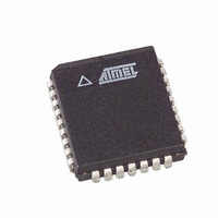
AT49LW080-33JC SL383 Atmel, AT49LW080-33JC SL383 Datasheet - Page 7

AT49LW080-33JC SL383
Manufacturer Part Number
AT49LW080-33JC SL383
Description
IC FLASH 8MBIT 33MHZ 32PLCC
Manufacturer
Atmel
Datasheet
1.AT49LW080-33JC.pdf
(34 pages)
Specifications of AT49LW080-33JC SL383
Format - Memory
FLASH
Memory Type
FLASH
Memory Size
8M (1M x 8)
Speed
33MHz
Interface
Parallel
Voltage - Supply
3 V ~ 3.6 V
Operating Temperature
0°C ~ 85°C
Package / Case
32-PLCC
Lead Free Status / RoHS Status
Contains lead / RoHS non-compliant
5.4
5.4.1
5.4.2
1966G–FLASH–3/05
Cycle Types
Preamble
Start
During sector erase or program, driving RST or INIT low will abort the operation underway, in
addition to causing a reset latency. Memory contents being altered are no longer valid, since the
data may be partially erased or programmed.
It is important to assert RST or INIT during system reset. When the system comes out of reset, it
will expect to read from the memory array of the device. If a system reset occurs with no FWH
reset (this will be hardware dependent), it is possible that proper CPU initialization will not occur
(the FWH memory may be providing status information instead of memory array data).
There are two types of cycles that are supported by the AT49LW080: FWH Memory Read and
FWH Memory Write. FWH Memory Read or Write cycles start with a preamble.
The preamble consists of a START, IDSEL, 28-bit Address and MSIZE fields. The preamble is
shown in
FWH[3:0]. For FWH Memory Read cycles, the START field must be 1101b; for FWH Memory
Write cycles, the START field must be 1110b. Following the START field is the IDSEL field. This
field acts like a chip select in that it indicates which device should respond to the current transac-
tion. The next seven clocks are the 28-bit address, which tell from where to begin reading or
writing in the selected device. Next, an MSIZE value of 0 indicates the master is requesting a
single byte.
Figure 5-1.
This one-clock field indicates the start of a cycle. It is valid on the last clock that FWH4 is sam-
pled low. The two start fields that are used for the cycle are shown in
that is sampled is not one of these values, then the cycle attempted is not an FWH memory
cycle. It may be a valid memory cycle that the FWH component may wish to decode, i.e., it may
be of the LPC memory cycle variety.
Table 5-2.
FWH[3:0]
1101b
1110b
FWH3 - FWH0
FWH4
Figure
CLK
FWH Memory Cycle Preamble
Start Fields
5-1. The preamble begins with FWH4 going low and a START field driven on
START
Indication
FWH Memory Read
FWH Memory Write
IDSEL
28-BIT ADDRESS
Table
AT49LW080
5-2. If the start field
MSIZE
7


