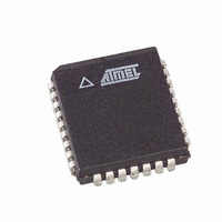
AT49LW080-33JC SL383 Atmel, AT49LW080-33JC SL383 Datasheet - Page 5

AT49LW080-33JC SL383
Manufacturer Part Number
AT49LW080-33JC SL383
Description
IC FLASH 8MBIT 33MHZ 32PLCC
Manufacturer
Atmel
Datasheet
1.AT49LW080-33JC.pdf
(34 pages)
Specifications of AT49LW080-33JC SL383
Format - Memory
FLASH
Memory Type
FLASH
Memory Size
8M (1M x 8)
Speed
33MHz
Interface
Parallel
Voltage - Supply
3 V ~ 3.6 V
Operating Temperature
0°C ~ 85°C
Package / Case
32-PLCC
Lead Free Status / RoHS Status
Contains lead / RoHS non-compliant
Table 4-1.
1966G–FLASH–3/05
I/O0 - I/O7
Symbol
A0 - A10
RY/BY
GNDa
GND
V
RFU
R/C
WP
WE
V
V
OE
NC
CCa
PP
CC
Pin Description (Continued)
OUTPUT
SUPPLY
SUPPLY
SUPPLY
SUPPLY
SUPPLY
INPUT
INPUT
INPUT
INPUT
INPUT
Type
I/O
FWH
X
X
X
X
X
X
X
X
Interface
A/A Mux
X
X
X
X
X
X
X
X
X
X
X
X
Name and Function
WRITE-PROTECT: When low, prevents programming or sector erase to all but the
highest addressable sectors (0 - 14), regardless of the state of the corresponding lock
registers. WP-high disables hardware write protection for these sectors, though register-
based protection still applies. The status of TBL does not affect the status of sector-
locking registers.
A/A Mux = A5
LOW-ORDER ADDRESS INPUTS: Inputs for low-order addresses during read and
write operations. Addresses are internally latched during a write cycle. For the A/A Mux
interface these addresses are latched by R/C and share the same pins as the high-
order address inputs.
DATA INPUT/OUTPUTS: These pins receive data and commands during write cycles
and transmit data during memory array and identifier code read cycles. Data pins float
to high-impedance when the chip is deselected or outputs are disabled. Data is
internally latched during a write cycle.
OUTPUT ENABLE: Gates the device’s outputs during a read cycle.
ROW-COLUMN ADDRESS SELECT: For the A/A Mux interface, this pin determines
whether the address pins are pointing to the row addresses, A0 - A10, or to the column
addresses, A11 - A19.
WRITE ENABLE: Controls writes to the array sectors. Addresses and data are latched
on the rising edge of the WE pulse.
SECTOR ERASE/PROGRAM POWER SUPPLY: For erasing array sectors or
programming data. V
altered. Sector erase or program with an invalid V
spurious results and should not be attempted. V
over the lifetime of the device.
DEVICE POWER SUPPLY: Internal detection automatically configures the device for
optimized read performance. Do no float any power pins. With V
attempts to the flash memory are inhibited. Device operations at invalid V
(see DC Characteristics) produce spurious results and should not be attempted.
GROUND: Do not float any ground pins.
ANALOG POWER SUPPLY: This supply should share the same system supply as V
ANALOG GROUND: Should be tied to same plane as GND.
RESERVED FOR FUTURE USE: These pins are reserved for future generations of this
product and should be connected accordingly. These pins may be left disconnected or
driven. If they are driven, the voltage levels should meet V
A/A Mux = I/O[7:4]
NO CONNECT: Pin may be driven or floated. If it is driven, the voltage levels should
meet V
READY/BUSY: Valid only in A/A Mux Mode. This output pin is a reflection of bit 7 in the
status register. This pin is used to determine sector erase or program completion.
IH
and V
IL
. No connects appear only on the 40-lead TSOP package.
PP
= 3.3V or 12V. With V
PP
PP
≤ V
PP
may only be held at 12V for 80 hours
PPLK
(see DC Characteristics) produces
, memory contents cannot be
IH
AT49LW080
and V
CC
IL
≤ V
requirements.
LKO
CC
, all write
voltages
CC
.
5


