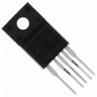
FSCQ1565RTYDTU Fairchild Semiconductor, FSCQ1565RTYDTU Datasheet - Page 15

FSCQ1565RTYDTU
Manufacturer Part Number
FSCQ1565RTYDTU
Description
IC SWIT PWM GREEN OVP HV TO220
Manufacturer
Fairchild Semiconductor
Datasheet
1.FSCQ1565RTYDTU.pdf
(45 pages)
Specifications of FSCQ1565RTYDTU
Output Isolation
Isolated
Frequency Range
18 ~ 22kHz
Voltage - Input
9 ~ 20 V
Voltage - Output
650V
Power (watts)
210W
Operating Temperature
25°C ~ 150°C
Package / Case
TO-220-5 Full Pack (Formed Leads)
Power Switch Family
FSCQ1565RT
Input Voltage
-0.3 to 20V
Power Switch On Resistance
530mOhm
Output Current
7.04A
Number Of Outputs
Single
Mounting
Through Hole
Supply Current
7mA
Package Type
TO-220F
Operating Temperature (min)
-25C
Operating Temperature (max)
85C
Operating Temperature Classification
Commercial
Pin Count
5 +Tab
Power Dissipation
75W
On Resistance (max)
0.53 Ohms
Maximum Operating Temperature
+ 85 C
Minimum Operating Temperature
- 25 C
Maximum Power Dissipation
75000 mW
Mounting Style
Through Hole
Supply Voltage (max)
20 V
Power Dissipation Pd
170W
No. Of Pins
5
Operating Temperature Range
-25°C To +85°C
Filter Terminals
Through Hole
Output Current Max
12A
Peak Reflow Compatible (260 C)
Yes
Rohs Compliant
Yes
Current Rating
8.0A
Leaded Process Compatible
Yes
Lead Free Status / RoHS Status
Lead free / RoHS Compliant
Other names
FSCQ1565RTYDTU_NL
FSCQ1565RTYDTU_NL
FSCQ1565RTYDTU_NL
Available stocks
Company
Part Number
Manufacturer
Quantity
Price
Company:
Part Number:
FSCQ1565RTYDTU
Manufacturer:
LITEON
Quantity:
1 500
Part Number:
FSCQ1565RTYDTU
Manufacturer:
FAIRCHILD/仙童
Quantity:
20 000
FSCQ-Series Rev. 1.1.2
The minimum drain voltage is indirectly detected by mon-
itoring the Vcc winding voltage as shown in Figure 6 and
8. Choose voltage dividers, R
peak voltage of the sync signal (V
OVP voltage (12V) to avoid triggering OVP in normal
operation. It is typical to set V
voltage by 3–4V. To detect the optimum time to turn on
MOSFET, the sync capacitor (C
mined so that T
8. The T
where L
former, and N
output winding and V
V
winding and Vcc winding, respectively, and C
sum of the output capacitance of the MOSFET and the
external capacitor, Cr.
V
T
Fa
V
I
T
V
ds
gs
R
ds
Q
co
are the diode forward voltage drops of the output
=
=
Figure 7. Quasi-Resonant Operation
=
R
R
m
N
----------------------------------------- - V
SY2
and T
a
is the primary side inductance of the trans-
L
m
s
V
C
R
Q
N
and N
o
SY
MOSFET
is the same with T
s
C
are given as, respectively:
+
I
eo
pk
V
Off
In
FO
Waveforms
CC
a
are the number of turns for the
V
-------- -
2.6
–
winding, respectively, V
co
V
V
Fa
RO
RO
MOSFET
sypk
SY1
--------------------------------- -
R
SY1
On
R
SY
and R
sypk
to be lower than OVP
Q
SY2
+
V
) should be deter-
as shown in Figure
DC
R
) is lower than the
SY2
SY2,
so that the
eo
Fo
is the
and
15
In general, the QRC has a limitation in a wide load range
application, since the switching frequency increases as
the output load decreases, resulting in a severe switch-
ing loss in the light load condition. To overcome this limi-
tation, the FSCQ-Series employs an extended quasi-
resonant switching operation. Figure 9 shows the mode
change between normal and extended quasi-resonant
operations. In the normal quasi-resonant operation, the
FSCQ-Series enters into the extended quasi-resonant
operation when the switching frequency exceeds 90kHz
as the load reduces. To reduce the switching frequency,
the MOSFET is turned on when the drain voltage
Figure 9. Extended Quasi-Resonant Operation
90kHz
45kHz
MOSFET Gate
V
V
ds
2V
sync
Switching
frequency
RO
ON
Figure 8. Normal Quasi-Resonant
Operation Waveforms
Extended QR operation
T
T
Q
R
Vrh (4.6V)
Vrf (2.6V)
V
Normal QR operation
sypk
ON
Output power
www.fairchildsemi.com


