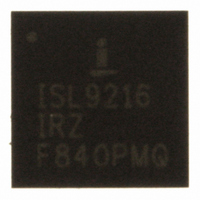
ISL9216IRZ Intersil, ISL9216IRZ Datasheet - Page 27

ISL9216IRZ
Manufacturer Part Number
ISL9216IRZ
Description
IC MULTI-CELL LI-ION PROT 32-QFN
Manufacturer
Intersil
Datasheet
1.ISL9216IRZ.pdf
(33 pages)
Specifications of ISL9216IRZ
Function
Battery Monitor
Battery Type
Lithium-Ion (Li-Ion)
Voltage - Supply
9.2 V ~ 31 V
Operating Temperature
-40°C ~ 85°C
Mounting Type
Surface Mount
Package / Case
32-VQFN Exposed Pad, 32-HVQFN, 32-SQFN, 32-DHVQFN
Lead Free Status / RoHS Status
Lead free / RoHS Compliant
Available stocks
Company
Part Number
Manufacturer
Quantity
Price
Company:
Part Number:
ISL9216IRZ
Manufacturer:
BROADCOM
Quantity:
1 000
Company:
Part Number:
ISL9216IRZ
Manufacturer:
Intersil
Quantity:
802
Part Number:
ISL9216IRZ
Manufacturer:
INTERSIL
Quantity:
20 000
When receiving data from the master, the value in the data
byte is transferred into the register specified by the address
byte on the falling edge of the clock following the 8th data bit.
After receiving the acknowledge after the data byte, the device
automatically increments the address. So, before sending the
stop bit, the master may send additional data to the device
without re-sending the slave and address bytes. After writing to
address 0AH, the address “wraps around’ to address 0.
Read Operations
Read operations are initiated in the same manner as write
operations with the host sending the address where the read
is to start (but no data). Then, the host sends an ACK, a
repeated start and the slave byte with the LSB = 1. After the
device acknowledges the slave byte, the device sends out
one bit of data for each master clock. After the slave sends 8
bits to the master, the master sends a NACK (Not
acknowledge) to the device to indicate that the data transfer
is complete, then the master sends a stop bit. See Figure 13.
After sending the eighth data bit to the master, the device
automatically increments its internal address pointer.
Therefore, the master, instead of sending a NACK and the
stop bit, can send additional clocks to read the contents of
the next register - without sending another slave and
address byte.
If the last address read or written is known, the master can
initiate a current address read. In this case, only the slave byte
is sent before data is returned. See Figure 13.
SDA BUS
SDA BUS
A
R
S
T
T
A
R
0 1 0 1
S
T
T
0 1 0 1
FIGURE 12. WRITE SEQUENCE
SLAVE
ISL9216: x = 0 [SLAVE BYTE = 50H]
ISL9217: x = 1 [SLAVE BYTE = 52H]
BYTE
SLAVE
BYTE
0
0 x
0
0 0
0
A
C
K
0
A
C
K
27
REGISTER
ADDRESS
REGISTER
ADDRESS
RANDOM READ
A
C
K
A
C
K
S
A
R
T
T
0 1 0 1
DATA
SLAVE
FIGURE 13. READ SEQUENCE
BYTE
ISL9216, ISL9217
0
0 0
ISL9208: SLAVE BYTE = 010100xH
A
C
K
O
S
T
P
1
A
C
K
DATA
Cascade Operation
When devices are cascaded, the lower device has the I
slave address of 0101 000x and the upper device has the
address 0101 001x (See Figure 14), but the operation of
cascaded devices is transparent to the microcontroller
master device.
The serial interface between cascaded ISL9216 and
ISL9217 devices has one clock and two data lines. There is
also a high voltage reference for this commication link. See
Figure 15. The interface lines are:
• SCLHV, which is a level shifted clock from the lower
• SDAOHV and SDAO, which send level shifted data out of
• SDAIHV and SDAI, which are level shifted inputs into the
• HVI2C (ISL9216), which is a reference voltage for the level
device (ISL9216) to the upper device (ISL9217);
the ISL9216 and ISL9217 (respectively); and
ISL9216 and ISL9217 (respectively).
shifted interface. This connects to the ISL9217 RGO pin.
SDA
SCL
1010 000x
N
A
C
K
ISL9216 SLAVE BYTE
ISL9217 SLAVE BYTE
S
O
P
T
FIGURE 15. I
FIGURE 14. DEVICE SLAVE BYTES
ISL9216
BLOCK
LEVEL
LEVEL
LEVEL
SHIFT
SHIFT
SHIFT
I
2
2
C
C CASCADED INTERFACE
A
R
S
T
T
CURRENT ADDRESS READ
0 1 0 1
0
0
SDAOHV
SLAVE
SDAIHV
BYTE
SCLHV
1
1
HVI2C
0
0
0
0 0
1
1
1
A
C
K
0
0
1010 001x
SDAI
SDAO
0
0
RGO
SCL
ISL9217
DATA
0
1
November 2, 2007
X
X
BLOCK
I
FN6488.1
2
N
A
C
K
C
2
O
C
S
T
P


