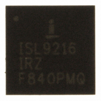
ISL9216IRZ Intersil, ISL9216IRZ Datasheet - Page 28

ISL9216IRZ
Manufacturer Part Number
ISL9216IRZ
Description
IC MULTI-CELL LI-ION PROT 32-QFN
Manufacturer
Intersil
Datasheet
1.ISL9216IRZ.pdf
(33 pages)
Specifications of ISL9216IRZ
Function
Battery Monitor
Battery Type
Lithium-Ion (Li-Ion)
Voltage - Supply
9.2 V ~ 31 V
Operating Temperature
-40°C ~ 85°C
Mounting Type
Surface Mount
Package / Case
32-VQFN Exposed Pad, 32-HVQFN, 32-SQFN, 32-DHVQFN
Lead Free Status / RoHS Status
Lead free / RoHS Compliant
Available stocks
Company
Part Number
Manufacturer
Quantity
Price
Company:
Part Number:
ISL9216IRZ
Manufacturer:
BROADCOM
Quantity:
1 000
Company:
Part Number:
ISL9216IRZ
Manufacturer:
Intersil
Quantity:
802
Part Number:
ISL9216IRZ
Manufacturer:
INTERSIL
Quantity:
20 000
When data is clocked into the ISL9216 through the I
is immediately transferred to the serial cascade port, so both
the ISL9216 and ISL9217 see the slave byte at the same
time. After the 8th slave bit, the device that receives the
correct slave byte sends an acknowledge, while the other
device ignores all subsequent data on the serial port until it
receives a stop bit. However, even though the ISL9216
ignores the data, it still passes it through to the ISL9217.
The SDAI and SDAO pins of the ISL9217 need to have pull-
up resistors of approximately 4.7kΩ, since the output drivers
are open-drain devices.
Register Protection
The Discharge Set, Charge Set, and Feature Set
configuration registers are write protected on initial power-
up. In order to write to these registers it is necessary to set a
bit to enable each one. These write enable bits are in the
Write Enable register (Address 08H).
CFET, DFET, Cell balancing outputs are all off.
circuits and temperature protection circuits are
conditions force power FETs and cell balance
active (Default). Overcurrent conditions force
Voltage and temperature monitoring circuits
power FETs to turn off. Over-temperature
Logic and registers are powered by RGO
Charge and discharge current protection
(Require external command to turn on)
MAIN OPERATING STATE
are awaiting external control.
Voltage Regulator is ON
outputs to turn off.
28
FIGURE 16. DEVICE OPERATION STATE MACHINE
Power Fails and one of the supplies, V
and V
I
2
I
CELL3
2
C interface is disabled. Biasing is disabled.
2
All registers set to default values (All “0”)
C interface is enabled. Biasing is enabled.
C port, it
ISL9216, ISL9217
[ISL9217 wake-up requires µC
POWER-DOWN STATE
WKUP goes above or below
Voltage Regulator is enabled.
do not meet minimum voltage requirements
threshold (edge triggered).
Or, SLEEP bit is set to ‘0’
POWER-UP STATE
command to ISL9216].
SLEEP bit is set to ‘1’
V
Write the FSETEN bit (Addr 8:bit 7) to “1” to change the data
in the Feature Set register (Address 7).
Write the CHSETEN bit (Addr 8:bit 6) to “1” to change the
data in the Feature Set register (Address 6).
Write the DISSETEN bit (Addr 8:bit 5) to “1” to change the
data in the Feature Set register (Address 5).
The microcontroller can reset these bits back to zero to
prevent inadvertent writes that change the operation of the
pack.
Operation State Machine
Figure 16 shows a device state machine which defines how
the ISL9216 and ISL9217 respond to various conditions.
CELL2
Power is applied and all of the supplies, V
CC
, and V
, V
CELL1
CELL3
, V
CFET, DFET, Cell balancing outputs are all off.
I
2
CELL2
Voltage and temperature monitoring circuits
Logic and registers are powered by V
C communication is active (if V
meet minimum voltage requirements
Charge and discharge current protection
is high enough to operate with external
,
Voltage Regulator is OFF
SLEEP STATE
Biasing is OFF
circuits all off.
device.)
are off.
CC
, V
CELL1
CELL1
,
CELL1
voltage
November 2, 2007
FN6488.1


